

10 Fundamentals of Bonding Technology and Process Materials …
267
Pad opening
Misalignment
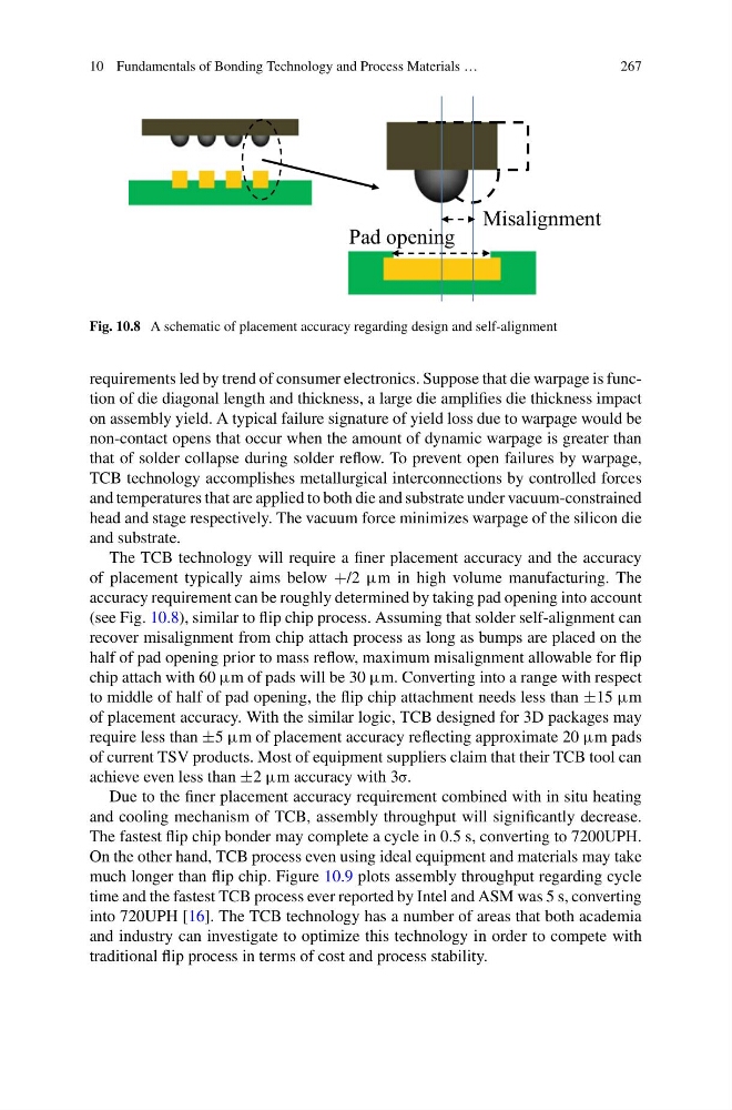
Fig. 10.8 A schematic of placement accuracy regarding design and self-alignment
requirements led by trend of consumer electronics. Suppose that die warpage is function of die diagonal length and thickness, a large die amplifies die thickness impact
on assembly yield. A typical failure signature of yield loss due to warpage would be
non-contact opens that occur when the amount of dynamic warpage is greater than
that of solder collapse during solder reflow. To prevent open failures by warpage,
TCB technology accomplishes metallurgical interconnections by controlled forces
and temperatures that are applied to both die and substrate under vacuum-constrained
head and stage respectively. The vacuum force minimizes warpage of the silicon die
and substrate.
The TCB technology will require a finer placement accuracy and the accuracy
of placement typically aims below +/2 μm in high volume manufacturing. The
accuracy requirement can be roughly determined by taking pad opening into account
(see Fig. 10.8), similar to flip chip process. Assuming that solder self-alignment can
recover misalignment from chip attach process as long as bumps are placed on the
half of pad opening prior to mass reflow, maximum misalignment allowable for flip
chip attach with 60 μm of pads will be 30 μm. Converting into a range with respect
to middle of half of pad opening, the flip chip attachment needs less than ±15 μm
of placement accuracy. With the similar logic, TCB designed for 3D packages may
require less than ±5 μm of placement accuracy reflecting approximate 20 μm pads
of current TSV products. Most of equipment suppliers claim that their TCB tool can
achieve even less than ±2 μm accuracy with 3σ.
Due to the finer placement accuracy requirement combined with in situ heating
and cooling mechanism of TCB, assembly throughput will significantly decrease.
The fastest flip chip bonder may complete a cycle in 0.5 s, converting to 7200UPH.
On the other hand, TCB process even using ideal equipment and materials may take
much longer than flip chip. Figure 10.9 plots assembly throughput regarding cycle
time and the fastest TCB process ever reported by Intel and ASM was 5 s, converting
into 720UPH [16]. The TCB technology has a number of areas that both academia
and industry can investigate to optimize this technology in order to compete with
traditional flip process in terms of cost and process stability.
267
Pad opening
Misalignment
Fig. 10.8 A schematic of placement accuracy regarding design and self-alignment
requirements led by trend of consumer electronics. Suppose that die warpage is function of die diagonal length and thickness, a large die amplifies die thickness impact
on assembly yield. A typical failure signature of yield loss due to warpage would be
non-contact opens that occur when the amount of dynamic warpage is greater than
that of solder collapse during solder reflow. To prevent open failures by warpage,
TCB technology accomplishes metallurgical interconnections by controlled forces
and temperatures that are applied to both die and substrate under vacuum-constrained
head and stage respectively. The vacuum force minimizes warpage of the silicon die
and substrate.
The TCB technology will require a finer placement accuracy and the accuracy
of placement typically aims below +/2 μm in high volume manufacturing. The
accuracy requirement can be roughly determined by taking pad opening into account
(see Fig. 10.8), similar to flip chip process. Assuming that solder self-alignment can
recover misalignment from chip attach process as long as bumps are placed on the
half of pad opening prior to mass reflow, maximum misalignment allowable for flip
chip attach with 60 μm of pads will be 30 μm. Converting into a range with respect
to middle of half of pad opening, the flip chip attachment needs less than ±15 μm
of placement accuracy. With the similar logic, TCB designed for 3D packages may
require less than ±5 μm of placement accuracy reflecting approximate 20 μm pads
of current TSV products. Most of equipment suppliers claim that their TCB tool can
achieve even less than ±2 μm accuracy with 3σ.
Due to the finer placement accuracy requirement combined with in situ heating
and cooling mechanism of TCB, assembly throughput will significantly decrease.
The fastest flip chip bonder may complete a cycle in 0.5 s, converting to 7200UPH.
On the other hand, TCB process even using ideal equipment and materials may take
much longer than flip chip. Figure 10.9 plots assembly throughput regarding cycle
time and the fastest TCB process ever reported by Intel and ASM was 5 s, converting
into 720UPH [16]. The TCB technology has a number of areas that both academia
and industry can investigate to optimize this technology in order to compete with
traditional flip process in terms of cost and process stability.