

266
S. Lee
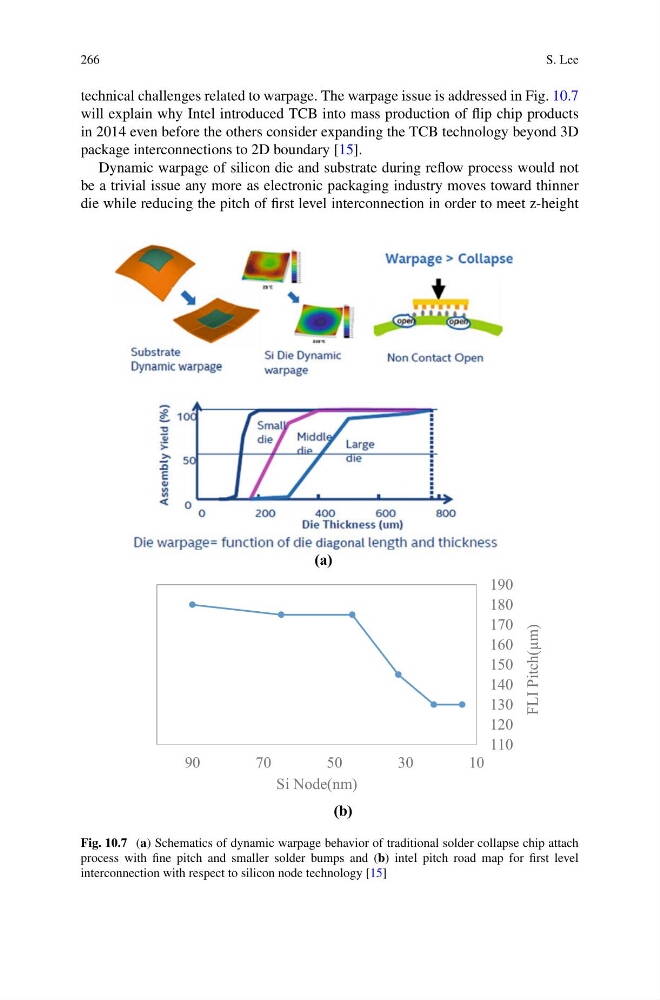
technical challenges related to warpage. The warpage issue is addressed in Fig. 10.7
will explain why Intel introduced TCB into mass production of flip chip products
in 2014 even before the others consider expanding the TCB technology beyond 3D
package interconnections to 2D boundary [15].
Dynamic warpage of silicon die and substrate during reflow process would not
be a trivial issue any more as electronic packaging industry moves toward thinner
die while reducing the pitch of first level interconnection in order to meet z-height
(b)
110
120
130
140
150
160
170
180
190
10
30
50
70
90
FLI Pitch(μm)
Si Node(nm)
(a)
Fig. 10.7 (a) Schematics of dynamic warpage behavior of traditional solder collapse chip attach
process with fine pitch and smaller solder bumps and (b) intel pitch road map for first level
interconnection with respect to silicon node technology [15]
S. Lee
technical challenges related to warpage. The warpage issue is addressed in Fig. 10.7
will explain why Intel introduced TCB into mass production of flip chip products
in 2014 even before the others consider expanding the TCB technology beyond 3D
package interconnections to 2D boundary [15].
Dynamic warpage of silicon die and substrate during reflow process would not
be a trivial issue any more as electronic packaging industry moves toward thinner
die while reducing the pitch of first level interconnection in order to meet z-height
(b)
110
120
130
140
150
160
170
180
190
10
30
50
70
90
FLI Pitch(μm)
Si Node(nm)
(a)
Fig. 10.7 (a) Schematics of dynamic warpage behavior of traditional solder collapse chip attach
process with fine pitch and smaller solder bumps and (b) intel pitch road map for first level
interconnection with respect to silicon node technology [15]