

262
S. Lee
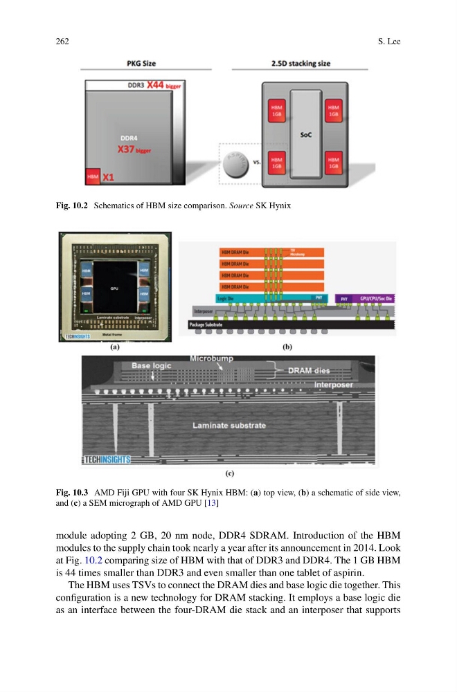
Fig. 10.2 Schematics of HBM size comparison. Source SK Hynix
Fig. 10.3 AMD Fiji GPU with four SK Hynix HBM: (a) top view, (b) a schematic of side view,
and (c) a SEM micrograph of AMD GPU [13]
module adopting 2 GB, 20 nm node, DDR4 SDRAM. Introduction of the HBM
modules to the supply chain took nearly a year after its announcement in 2014. Look
at Fig. 10.2 comparing size of HBM with that of DDR3 and DDR4. The 1 GB HBM
is 44 times smaller than DDR3 and even smaller than one tablet of aspirin.
The HBM uses TSVs to connect the DRAM dies and base logic die together. This
configuration is a new technology for DRAM stacking. It employs a base logic die
as an interface between the four-DRAM die stack and an interposer that supports
S. Lee
Fig. 10.2 Schematics of HBM size comparison. Source SK Hynix
Fig. 10.3 AMD Fiji GPU with four SK Hynix HBM: (a) top view, (b) a schematic of side view,
and (c) a SEM micrograph of AMD GPU [13]
module adopting 2 GB, 20 nm node, DDR4 SDRAM. Introduction of the HBM
modules to the supply chain took nearly a year after its announcement in 2014. Look
at Fig. 10.2 comparing size of HBM with that of DDR3 and DDR4. The 1 GB HBM
is 44 times smaller than DDR3 and even smaller than one tablet of aspirin.
The HBM uses TSVs to connect the DRAM dies and base logic die together. This
configuration is a new technology for DRAM stacking. It employs a base logic die
as an interface between the four-DRAM die stack and an interposer that supports