

10 Fundamentals of Bonding Technology and Process Materials …
261
exhibit high warpage even at room temperature and the amount of warpage will
exceed the limit of traditional mass reflow process. Due to the warpage challenge,
Intel Corporation introduced TCB technology in 2014 for their high volume manufacturing process of 130 μm pitch and 22 nm nodes, flip chip architecture to be ready
for all foreseen product configurations [11].
This session begins with an overview of the current 2.5/3D commercial products.
Then, the discussion compares TCB technology with traditional flip chip bonding
process using mass reflow. The comparison will address basic concepts of assembly
process in relation to engineering sciences as well as consider process limitations
associated with package design and equipment. Then fundamentals of process materials will be discussed in detail to understand key parameters of material selection and
to compare the pros and cons of each material. Thus, background session will provide
the essential fundamental science and engineering principles required to explore
2.5/3D packaging bonding technology, including a comprehension of its building
blocks; the association between those building blocks and package configurations;
and the selection of process materials relevant to package structure.
10.2.1 Overview of 3D Package Configuration
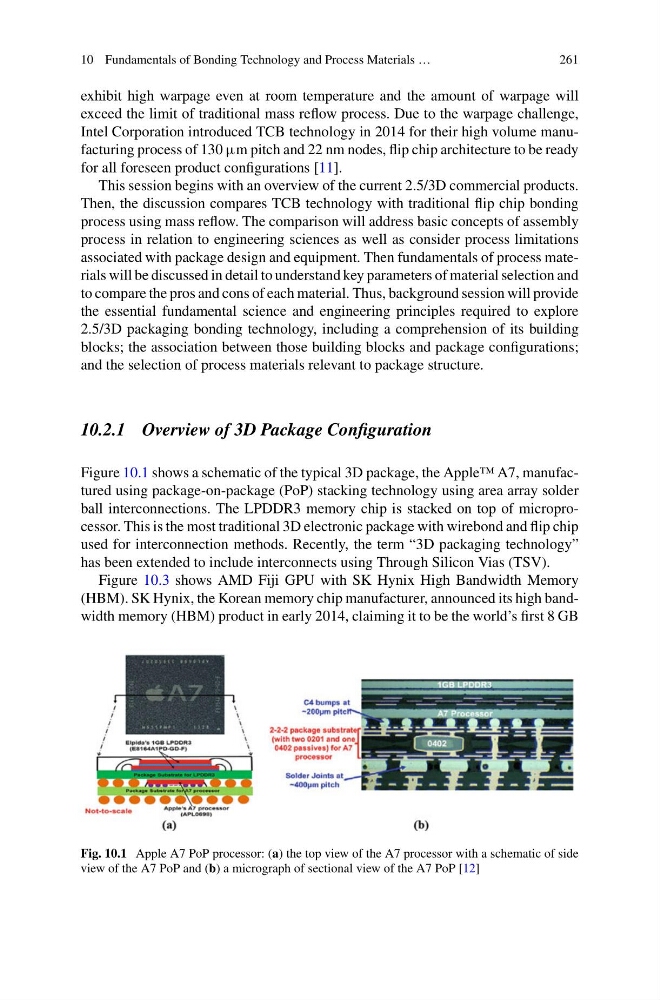
Figure 10.1 shows a schematic of the typical 3D package, the Apple™ A7, manufactured using package-on-package (PoP) stacking technology using area array solder
ball interconnections. The LPDDR3 memory chip is stacked on top of microprocessor. This is the most traditional 3D electronic package with wirebond and flip chip
used for interconnection methods. Recently, the term “3D packaging technology”
has been extended to include interconnects using Through Silicon Vias (TSV).
Figure 10.3 shows AMD Fiji GPU with SK Hynix High Bandwidth Memory
(HBM). SK Hynix, the Korean memory chip manufacturer, announced its high bandwidth memory (HBM) product in early 2014, claiming it to be the world’s first 8 GB
Fig. 10.1 Apple A7 PoP processor: (a) the top view of the A7 processor with a schematic of side
view of the A7 PoP and (b) a micrograph of sectional view of the A7 PoP [12]
261
exhibit high warpage even at room temperature and the amount of warpage will
exceed the limit of traditional mass reflow process. Due to the warpage challenge,
Intel Corporation introduced TCB technology in 2014 for their high volume manufacturing process of 130 μm pitch and 22 nm nodes, flip chip architecture to be ready
for all foreseen product configurations [11].
This session begins with an overview of the current 2.5/3D commercial products.
Then, the discussion compares TCB technology with traditional flip chip bonding
process using mass reflow. The comparison will address basic concepts of assembly
process in relation to engineering sciences as well as consider process limitations
associated with package design and equipment. Then fundamentals of process materials will be discussed in detail to understand key parameters of material selection and
to compare the pros and cons of each material. Thus, background session will provide
the essential fundamental science and engineering principles required to explore
2.5/3D packaging bonding technology, including a comprehension of its building
blocks; the association between those building blocks and package configurations;
and the selection of process materials relevant to package structure.
10.2.1 Overview of 3D Package Configuration
Figure 10.1 shows a schematic of the typical 3D package, the Apple™ A7, manufactured using package-on-package (PoP) stacking technology using area array solder
ball interconnections. The LPDDR3 memory chip is stacked on top of microprocessor. This is the most traditional 3D electronic package with wirebond and flip chip
used for interconnection methods. Recently, the term “3D packaging technology”
has been extended to include interconnects using Through Silicon Vias (TSV).
Figure 10.3 shows AMD Fiji GPU with SK Hynix High Bandwidth Memory
(HBM). SK Hynix, the Korean memory chip manufacturer, announced its high bandwidth memory (HBM) product in early 2014, claiming it to be the world’s first 8 GB
Fig. 10.1 Apple A7 PoP processor: (a) the top view of the A7 processor with a schematic of side
view of the A7 PoP and (b) a micrograph of sectional view of the A7 PoP [12]