

10 Fundamentals of Bonding Technology and Process Materials …
263
both the HBM modules and the AMD GPU. The HBM can be a 3D package, while
the laterally spaced layouts for the GPU and HBM modules on the interposer would
give it a 2.5D package designation.
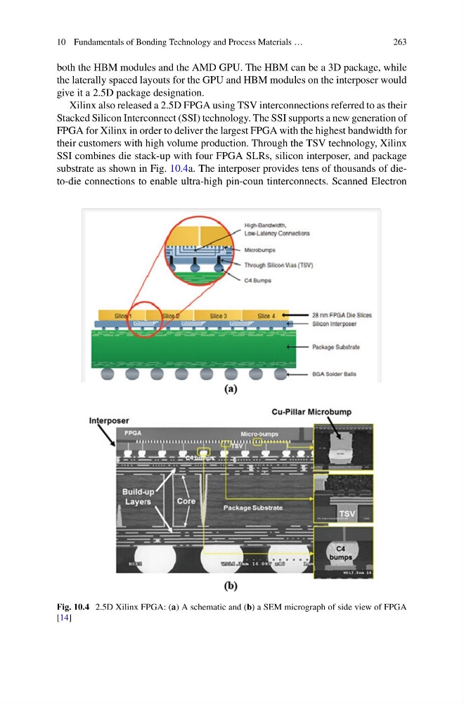
Xilinx also released a 2.5D FPGA using TSV interconnections referred to as their
Stacked Silicon Interconnect (SSI) technology. The SSI supports a new generation of
FPGA for Xilinx in order to deliver the largest FPGA with the highest bandwidth for
their customers with high volume production. Through the TSV technology, Xilinx
SSI combines die stack-up with four FPGA SLRs, silicon interposer, and package
substrate as shown in Fig. 10.4a. The interposer provides tens of thousands of dieto-die connections to enable ultra-high pin-coun tinterconnects. Scanned Electron
Fig. 10.4 2.5D Xilinx FPGA: (a) A schematic and (b) a SEM micrograph of side view of FPGA
[14]
263
both the HBM modules and the AMD GPU. The HBM can be a 3D package, while
the laterally spaced layouts for the GPU and HBM modules on the interposer would
give it a 2.5D package designation.
Xilinx also released a 2.5D FPGA using TSV interconnections referred to as their
Stacked Silicon Interconnect (SSI) technology. The SSI supports a new generation of
FPGA for Xilinx in order to deliver the largest FPGA with the highest bandwidth for
their customers with high volume production. Through the TSV technology, Xilinx
SSI combines die stack-up with four FPGA SLRs, silicon interposer, and package
substrate as shown in Fig. 10.4a. The interposer provides tens of thousands of dieto-die connections to enable ultra-high pin-coun tinterconnects. Scanned Electron
Fig. 10.4 2.5D Xilinx FPGA: (a) A schematic and (b) a SEM micrograph of side view of FPGA
[14]