

8
Y. Li and D. Goyal
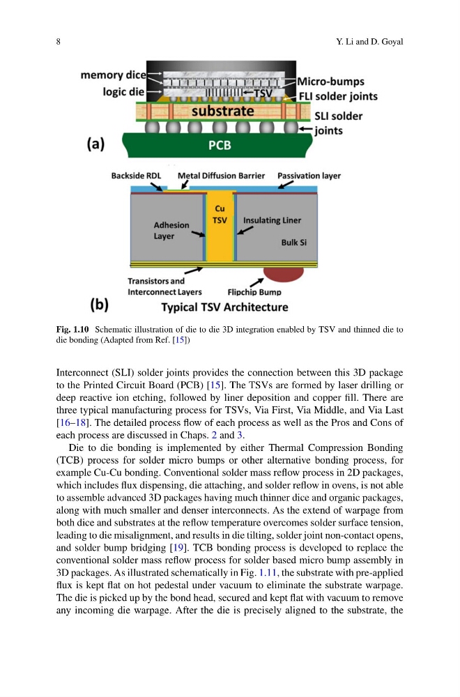
Fig. 1.10 Schematic illustration of die to die 3D integration enabled by TSV and thinned die to
die bonding (Adapted from Ref. [15])
Interconnect (SLI) solder joints provides the connection between this 3D package
to the Printed Circuit Board (PCB) [15]. The TSVs are formed by laser drilling or
deep reactive ion etching, followed by liner deposition and copper fill. There are
three typical manufacturing process for TSVs, Via First, Via Middle, and Via Last
[16–18]. The detailed process flow of each process as well as the Pros and Cons of
each process are discussed in Chaps. 2 and 3.
Die to die bonding is implemented by either Thermal Compression Bonding
(TCB) process for solder micro bumps or other alternative bonding process, for
example Cu-Cu bonding. Conventional solder mass reflow process in 2D packages,
which includes flux dispensing, die attaching, and solder reflow in ovens, is not able
to assemble advanced 3D packages having much thinner dice and organic packages,
along with much smaller and denser interconnects. As the extend of warpage from
both dice and substrates at the reflow temperature overcomes solder surface tension,
leading to die misalignment, and results in die tilting, solder joint non-contact opens,
and solder bump bridging [19]. TCB bonding process is developed to replace the
conventional solder mass reflow process for solder based micro bump assembly in
3D packages. As illustrated schematically in Fig. 1.11, the substrate with pre-applied
flux is kept flat on hot pedestal under vacuum to eliminate the substrate warpage.
The die is picked up by the bond head, secured and kept flat with vacuum to remove
any incoming die warpage. After the die is precisely aligned to the substrate, the
Y. Li and D. Goyal
Fig. 1.10 Schematic illustration of die to die 3D integration enabled by TSV and thinned die to
die bonding (Adapted from Ref. [15])
Interconnect (SLI) solder joints provides the connection between this 3D package
to the Printed Circuit Board (PCB) [15]. The TSVs are formed by laser drilling or
deep reactive ion etching, followed by liner deposition and copper fill. There are
three typical manufacturing process for TSVs, Via First, Via Middle, and Via Last
[16–18]. The detailed process flow of each process as well as the Pros and Cons of
each process are discussed in Chaps. 2 and 3.
Die to die bonding is implemented by either Thermal Compression Bonding
(TCB) process for solder micro bumps or other alternative bonding process, for
example Cu-Cu bonding. Conventional solder mass reflow process in 2D packages,
which includes flux dispensing, die attaching, and solder reflow in ovens, is not able
to assemble advanced 3D packages having much thinner dice and organic packages,
along with much smaller and denser interconnects. As the extend of warpage from
both dice and substrates at the reflow temperature overcomes solder surface tension,
leading to die misalignment, and results in die tilting, solder joint non-contact opens,
and solder bump bridging [19]. TCB bonding process is developed to replace the
conventional solder mass reflow process for solder based micro bump assembly in
3D packages. As illustrated schematically in Fig. 1.11, the substrate with pre-applied
flux is kept flat on hot pedestal under vacuum to eliminate the substrate warpage.
The die is picked up by the bond head, secured and kept flat with vacuum to remove
any incoming die warpage. After the die is precisely aligned to the substrate, the