

1 Introduction to 3D Microelectronic Packaging
7
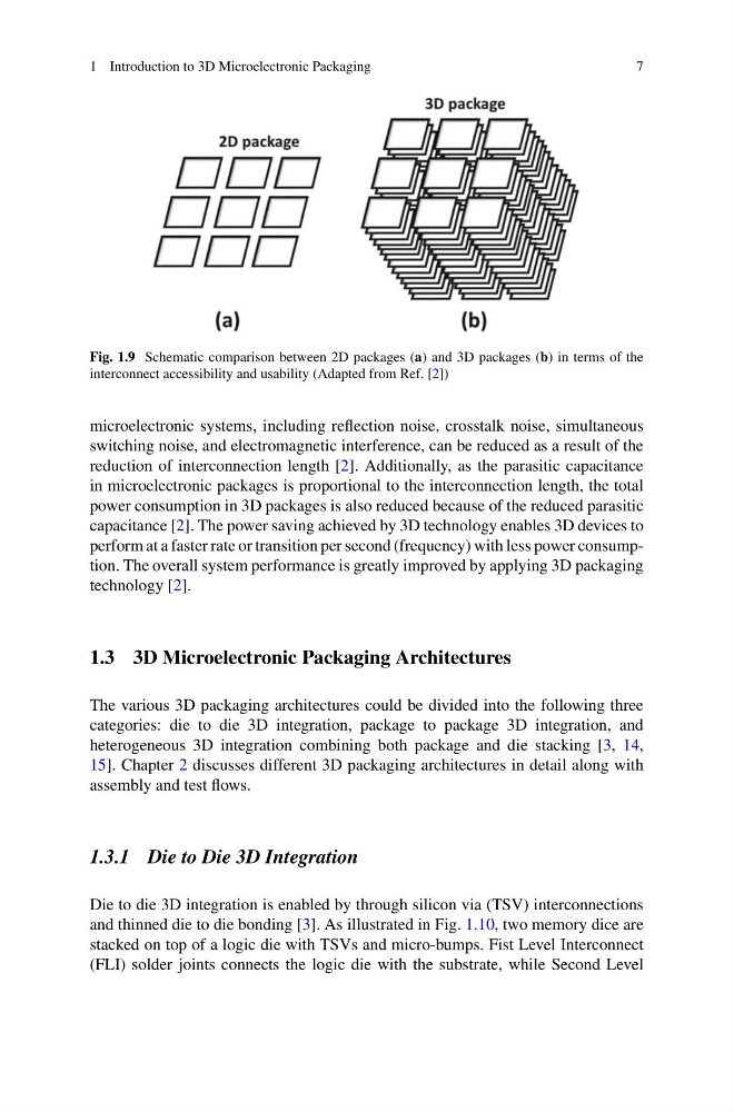
Fig. 1.9 Schematic comparison between 2D packages (a) and 3D packages (b) in terms of the
interconnect accessibility and usability (Adapted from Ref. [2])
microelectronic systems, including reflection noise, crosstalk noise, simultaneous
switching noise, and electromagnetic interference, can be reduced as a result of the
reduction of interconnection length [2]. Additionally, as the parasitic capacitance
in microelectronic packages is proportional to the interconnection length, the total
power consumption in 3D packages is also reduced because of the reduced parasitic
capacitance [2]. The power saving achieved by 3D technology enables 3D devices to
perform at a faster rate or transition per second (frequency) with less power consumption. The overall system performance is greatly improved by applying 3D packaging
technology [2].
1.3 3D Microelectronic Packaging Architectures
The various 3D packaging architectures could be divided into the following three
categories: die to die 3D integration, package to package 3D integration, and
heterogeneous 3D integration combining both package and die stacking [3, 14,
15]. Chapter 2 discusses different 3D packaging architectures in detail along with
assembly and test flows.
1.3.1 Die to Die 3D Integration
Die to die 3D integration is enabled by through silicon via (TSV) interconnections
and thinned die to die bonding [3]. As illustrated in Fig. 1.10, two memory dice are
stacked on top of a logic die with TSVs and micro-bumps. Fist Level Interconnect
(FLI) solder joints connects the logic die with the substrate, while Second Level
7
Fig. 1.9 Schematic comparison between 2D packages (a) and 3D packages (b) in terms of the
interconnect accessibility and usability (Adapted from Ref. [2])
microelectronic systems, including reflection noise, crosstalk noise, simultaneous
switching noise, and electromagnetic interference, can be reduced as a result of the
reduction of interconnection length [2]. Additionally, as the parasitic capacitance
in microelectronic packages is proportional to the interconnection length, the total
power consumption in 3D packages is also reduced because of the reduced parasitic
capacitance [2]. The power saving achieved by 3D technology enables 3D devices to
perform at a faster rate or transition per second (frequency) with less power consumption. The overall system performance is greatly improved by applying 3D packaging
technology [2].
1.3 3D Microelectronic Packaging Architectures
The various 3D packaging architectures could be divided into the following three
categories: die to die 3D integration, package to package 3D integration, and
heterogeneous 3D integration combining both package and die stacking [3, 14,
15]. Chapter 2 discusses different 3D packaging architectures in detail along with
assembly and test flows.
1.3.1 Die to Die 3D Integration
Die to die 3D integration is enabled by through silicon via (TSV) interconnections
and thinned die to die bonding [3]. As illustrated in Fig. 1.10, two memory dice are
stacked on top of a logic die with TSVs and micro-bumps. Fist Level Interconnect
(FLI) solder joints connects the logic die with the substrate, while Second Level