

6
Y. Li and D. Goyal
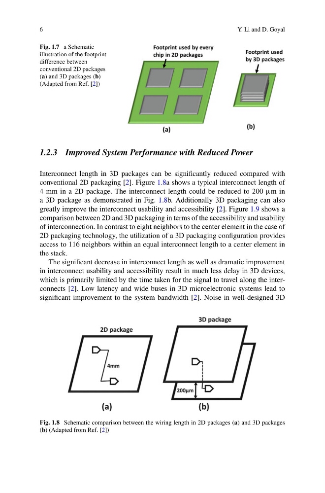
Fig. 1.7 a Schematic
illustration of the footprint
difference between
conventional 2D packages
(a) and 3D packages (b)
(Adapted from Ref. [2])
1.2.3 Improved System Performance with Reduced Power
Interconnect length in 3D packages can be significantly reduced compared with
conventional 2D packaging [2]. Figure 1.8a shows a typical interconnect length of
4 mm in a 2D package. The interconnect length could be reduced to 200 µm in
a 3D package as demonstrated in Fig. 1.8b. Additionally 3D packaging can also
greatly improve the interconnect usability and accessibility [2]. Figure 1.9 shows a
comparison between 2D and 3D packaging in terms of the accessibility and usability
of interconnection. In contrast to eight neighbors to the center element in the case of
2D packaging technology, the utilization of a 3D packaging configuration provides
access to 116 neighbors within an equal interconnect length to a center element in
the stack.
The significant decrease in interconnect length as well as dramatic improvement
in interconnect usability and accessibility result in much less delay in 3D devices,
which is primarily limited by the time taken for the signal to travel along the interconnects [2]. Low latency and wide buses in 3D microelectronic systems lead to
significant improvement to the system bandwidth [2]. Noise in well-designed 3D
Fig. 1.8 Schematic comparison between the wiring length in 2D packages (a) and 3D packages
(b) (Adapted from Ref. [2])
Y. Li and D. Goyal
Fig. 1.7 a Schematic
illustration of the footprint
difference between
conventional 2D packages
(a) and 3D packages (b)
(Adapted from Ref. [2])
1.2.3 Improved System Performance with Reduced Power
Interconnect length in 3D packages can be significantly reduced compared with
conventional 2D packaging [2]. Figure 1.8a shows a typical interconnect length of
4 mm in a 2D package. The interconnect length could be reduced to 200 µm in
a 3D package as demonstrated in Fig. 1.8b. Additionally 3D packaging can also
greatly improve the interconnect usability and accessibility [2]. Figure 1.9 shows a
comparison between 2D and 3D packaging in terms of the accessibility and usability
of interconnection. In contrast to eight neighbors to the center element in the case of
2D packaging technology, the utilization of a 3D packaging configuration provides
access to 116 neighbors within an equal interconnect length to a center element in
the stack.
The significant decrease in interconnect length as well as dramatic improvement
in interconnect usability and accessibility result in much less delay in 3D devices,
which is primarily limited by the time taken for the signal to travel along the interconnects [2]. Low latency and wide buses in 3D microelectronic systems lead to
significant improvement to the system bandwidth [2]. Noise in well-designed 3D
Fig. 1.8 Schematic comparison between the wiring length in 2D packages (a) and 3D packages
(b) (Adapted from Ref. [2])