

1 Introduction to 3D Microelectronic Packaging
5
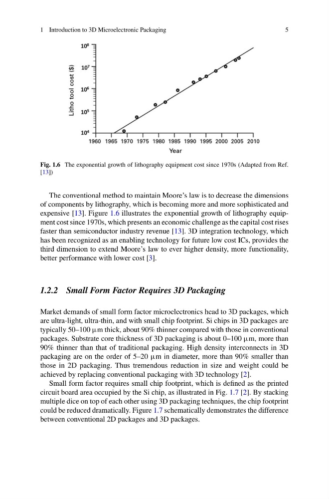
Fig. 1.6 The exponential growth of lithography equipment cost since 1970s (Adapted from Ref.
[13])
The conventional method to maintain Moore’s law is to decrease the dimensions
of components by lithography, which is becoming more and more sophisticated and
expensive [13]. Figure 1.6 illustrates the exponential growth of lithography equipment cost since 1970s, which presents an economic challenge as the capital cost rises
faster than semiconductor industry revenue [13]. 3D integration technology, which
has been recognized as an enabling technology for future low cost ICs, provides the
third dimension to extend Moore’s law to ever higher density, more functionality,
better performance with lower cost [3].
1.2.2 Small Form Factor Requires 3D Packaging
Market demands of small form factor microelectronics head to 3D packages, which
are ultra-light, ultra-thin, and with small chip footprint. Si chips in 3D packages are
typically 50–100 µm thick, about 90% thinner compared with those in conventional
packages. Substrate core thickness of 3D packaging is about 0–100 µm, more than
90% thinner than that of traditional packaging. High density interconnects in 3D
packaging are on the order of 5–20 µm in diameter, more than 90% smaller than
those in 2D packaging. Thus tremendous reduction in size and weight could be
achieved by replacing conventional packaging with 3D technology [2].
Small form factor requires small chip footprint, which is defined as the printed
circuit board area occupied by the Si chip, as illustrated in Fig. 1.7 [2]. By stacking
multiple dice on top of each other using 3D packaging techniques, the chip footprint
could be reduced dramatically. Figure 1.7 schematically demonstrates the difference
between conventional 2D packages and 3D packages.
5
Fig. 1.6 The exponential growth of lithography equipment cost since 1970s (Adapted from Ref.
[13])
The conventional method to maintain Moore’s law is to decrease the dimensions
of components by lithography, which is becoming more and more sophisticated and
expensive [13]. Figure 1.6 illustrates the exponential growth of lithography equipment cost since 1970s, which presents an economic challenge as the capital cost rises
faster than semiconductor industry revenue [13]. 3D integration technology, which
has been recognized as an enabling technology for future low cost ICs, provides the
third dimension to extend Moore’s law to ever higher density, more functionality,
better performance with lower cost [3].
1.2.2 Small Form Factor Requires 3D Packaging
Market demands of small form factor microelectronics head to 3D packages, which
are ultra-light, ultra-thin, and with small chip footprint. Si chips in 3D packages are
typically 50–100 µm thick, about 90% thinner compared with those in conventional
packages. Substrate core thickness of 3D packaging is about 0–100 µm, more than
90% thinner than that of traditional packaging. High density interconnects in 3D
packaging are on the order of 5–20 µm in diameter, more than 90% smaller than
those in 2D packaging. Thus tremendous reduction in size and weight could be
achieved by replacing conventional packaging with 3D technology [2].
Small form factor requires small chip footprint, which is defined as the printed
circuit board area occupied by the Si chip, as illustrated in Fig. 1.7 [2]. By stacking
multiple dice on top of each other using 3D packaging techniques, the chip footprint
could be reduced dramatically. Figure 1.7 schematically demonstrates the difference
between conventional 2D packages and 3D packages.