

8 Direct Cu to Cu Bonding and Alternative Bonding Techniques …
219
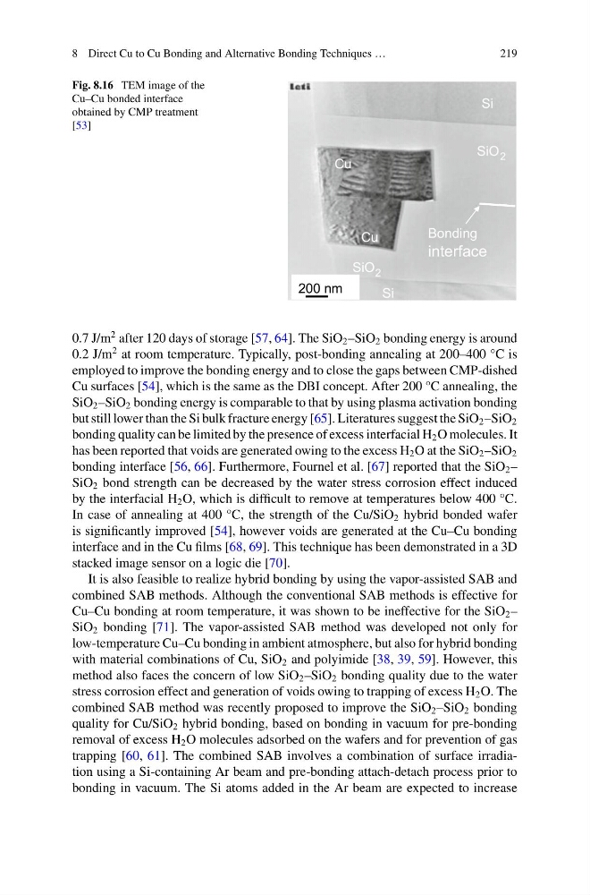
Fig. 8.16 TEM image of the
Cu–Cu bonded interface
obtained by CMP treatment
[53]
2
2
interface
200 nm
Si
SiO
SiO
Cu
Cu
Bonding
Si
200 nm
0.7 J/m
2 after 120 days of storage [57, 64]. The SiO 2 –SiO 2 bonding energy is around
0.2 J/m
2 at room temperature. Typically, post-bonding annealing at 200–400 °C is
employed to improve the bonding energy and to close the gaps between CMP-dished
Cu surfaces [54], which is the same as the DBI concept. After 200 °C annealing, the
SiO 2 –SiO 2 bonding energy is comparable to that by using plasma activation bonding
but still lower than the Si bulk fracture energy [65]. Literatures suggest the SiO 2 –SiO 2
bonding quality can be limited by the presence of excess interfacial H 2 O molecules. It
has been reported that voids are generated owing to the excess H 2 O at the SiO 2 –SiO 2
bonding interface [56, 66]. Furthermore, Fournel et al. [67] reported that the SiO 2 –
SiO 2 bond strength can be decreased by the water stress corrosion effect induced
by the interfacial H 2 O, which is difficult to remove at temperatures below 400 °C.
In case of annealing at 400 °C, the strength of the Cu/SiO 2 hybrid bonded wafer
is significantly improved [54], however voids are generated at the Cu–Cu bonding
interface and in the Cu films [68, 69]. This technique has been demonstrated in a 3D
stacked image sensor on a logic die [70].
It is also feasible to realize hybrid bonding by using the vapor-assisted SAB and
combined SAB methods. Although the conventional SAB methods is effective for
Cu–Cu bonding at room temperature, it was shown to be ineffective for the SiO 2 –
SiO 2 bonding [71]. The vapor-assisted SAB method was developed not only for
low-temperature Cu–Cu bonding in ambient atmosphere, but also for hybrid bonding
with material combinations of Cu, SiO 2 and polyimide [38, 39, 59]. However, this
method also faces the concern of low SiO 2 –SiO 2 bonding quality due to the water
stress corrosion effect and generation of voids owing to trapping of excess H 2 O. The
combined SAB method was recently proposed to improve the SiO 2 –SiO 2 bonding
quality for Cu/SiO 2 hybrid bonding, based on bonding in vacuum for pre-bonding
removal of excess H 2 O molecules adsorbed on the wafers and for prevention of gas
trapping [60, 61]. The combined SAB involves a combination of surface irradiation using a Si-containing Ar beam and pre-bonding attach-detach process prior to
bonding in vacuum. The Si atoms added in the Ar beam are expected to increase
219
Fig. 8.16 TEM image of the
Cu–Cu bonded interface
obtained by CMP treatment
[53]
2
2
interface
200 nm
Si
SiO
SiO
Cu
Cu
Bonding
Si
200 nm
0.7 J/m
2 after 120 days of storage [57, 64]. The SiO 2 –SiO 2 bonding energy is around
0.2 J/m
2 at room temperature. Typically, post-bonding annealing at 200–400 °C is
employed to improve the bonding energy and to close the gaps between CMP-dished
Cu surfaces [54], which is the same as the DBI concept. After 200 °C annealing, the
SiO 2 –SiO 2 bonding energy is comparable to that by using plasma activation bonding
but still lower than the Si bulk fracture energy [65]. Literatures suggest the SiO 2 –SiO 2
bonding quality can be limited by the presence of excess interfacial H 2 O molecules. It
has been reported that voids are generated owing to the excess H 2 O at the SiO 2 –SiO 2
bonding interface [56, 66]. Furthermore, Fournel et al. [67] reported that the SiO 2 –
SiO 2 bond strength can be decreased by the water stress corrosion effect induced
by the interfacial H 2 O, which is difficult to remove at temperatures below 400 °C.
In case of annealing at 400 °C, the strength of the Cu/SiO 2 hybrid bonded wafer
is significantly improved [54], however voids are generated at the Cu–Cu bonding
interface and in the Cu films [68, 69]. This technique has been demonstrated in a 3D
stacked image sensor on a logic die [70].
It is also feasible to realize hybrid bonding by using the vapor-assisted SAB and
combined SAB methods. Although the conventional SAB methods is effective for
Cu–Cu bonding at room temperature, it was shown to be ineffective for the SiO 2 –
SiO 2 bonding [71]. The vapor-assisted SAB method was developed not only for
low-temperature Cu–Cu bonding in ambient atmosphere, but also for hybrid bonding
with material combinations of Cu, SiO 2 and polyimide [38, 39, 59]. However, this
method also faces the concern of low SiO 2 –SiO 2 bonding quality due to the water
stress corrosion effect and generation of voids owing to trapping of excess H 2 O. The
combined SAB method was recently proposed to improve the SiO 2 –SiO 2 bonding
quality for Cu/SiO 2 hybrid bonding, based on bonding in vacuum for pre-bonding
removal of excess H 2 O molecules adsorbed on the wafers and for prevention of gas
trapping [60, 61]. The combined SAB involves a combination of surface irradiation using a Si-containing Ar beam and pre-bonding attach-detach process prior to
bonding in vacuum. The Si atoms added in the Ar beam are expected to increase