

218
T. Suga et al.
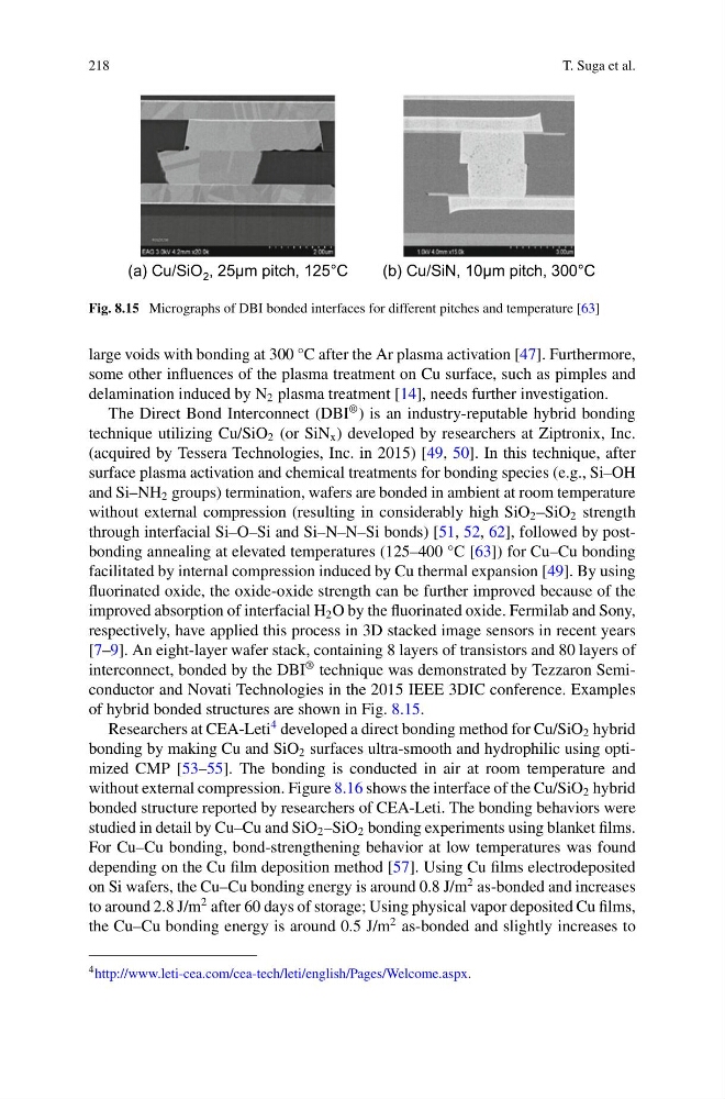
(a) Cu/SiO 2 , 25μm pitch, 125°C
(b) Cu/SiN, 10μm pitch, 300°C
Fig. 8.15 Micrographs of DBI bonded interfaces for different pitches and temperature [63]
large voids with bonding at 300 °C after the Ar plasma activation [47]. Furthermore,
some other influences of the plasma treatment on Cu surface, such as pimples and
delamination induced by N 2 plasma treatment [14], needs further investigation.
The Direct Bond Interconnect (DBI
® ) is an industry-reputable hybrid bonding
technique utilizing Cu/SiO 2 (or SiN x ) developed by researchers at Ziptronix, Inc.
(acquired by Tessera Technologies, Inc. in 2015) [49, 50]. In this technique, after
surface plasma activation and chemical treatments for bonding species (e.g., Si–OH
and Si–NH 2 groups) termination, wafers are bonded in ambient at room temperature
without external compression (resulting in considerably high SiO 2 –SiO 2 strength
through interfacial Si–O–Si and Si–N–N–Si bonds) [51, 52, 62], followed by postbonding annealing at elevated temperatures (125–400 °C [63]) for Cu–Cu bonding
facilitated by internal compression induced by Cu thermal expansion [49]. By using
fluorinated oxide, the oxide-oxide strength can be further improved because of the
improved absorption of interfacial H 2 O by the fluorinated oxide. Fermilab and Sony,
respectively, have applied this process in 3D stacked image sensors in recent years
[7–9]. An eight-layer wafer stack, containing 8 layers of transistors and 80 layers of
interconnect, bonded by the DBI
® technique was demonstrated by Tezzaron Semiconductor and Novati Technologies in the 2015 IEEE 3DIC conference. Examples
of hybrid bonded structures are shown in Fig. 8.15.
Researchers at CEA-Leti
4 developed a direct bonding method for Cu/SiO 2 hybrid
bonding by making Cu and SiO 2 surfaces ultra-smooth and hydrophilic using optimized CMP [53–55]. The bonding is conducted in air at room temperature and
without external compression. Figure 8.16 shows the interface of the Cu/SiO 2 hybrid
bonded structure reported by researchers of CEA-Leti. The bonding behaviors were
studied in detail by Cu–Cu and SiO 2 –SiO 2 bonding experiments using blanket films.
For Cu–Cu bonding, bond-strengthening behavior at low temperatures was found
depending on the Cu film deposition method [57]. Using Cu films electrodeposited
on Si wafers, the Cu–Cu bonding energy is around 0.8 J/m
2 as-bonded and increases
to around 2.8 J/m
2 after 60 days of storage; Using physical vapor deposited Cu films,
the Cu–Cu bonding energy is around 0.5 J/m
2 as-bonded and slightly increases to
4 http://www.leti-cea.com/cea-tech/leti/english/Pages/Welcome.aspx.
T. Suga et al.
(a) Cu/SiO 2 , 25μm pitch, 125°C
(b) Cu/SiN, 10μm pitch, 300°C
Fig. 8.15 Micrographs of DBI bonded interfaces for different pitches and temperature [63]
large voids with bonding at 300 °C after the Ar plasma activation [47]. Furthermore,
some other influences of the plasma treatment on Cu surface, such as pimples and
delamination induced by N 2 plasma treatment [14], needs further investigation.
The Direct Bond Interconnect (DBI
® ) is an industry-reputable hybrid bonding
technique utilizing Cu/SiO 2 (or SiN x ) developed by researchers at Ziptronix, Inc.
(acquired by Tessera Technologies, Inc. in 2015) [49, 50]. In this technique, after
surface plasma activation and chemical treatments for bonding species (e.g., Si–OH
and Si–NH 2 groups) termination, wafers are bonded in ambient at room temperature
without external compression (resulting in considerably high SiO 2 –SiO 2 strength
through interfacial Si–O–Si and Si–N–N–Si bonds) [51, 52, 62], followed by postbonding annealing at elevated temperatures (125–400 °C [63]) for Cu–Cu bonding
facilitated by internal compression induced by Cu thermal expansion [49]. By using
fluorinated oxide, the oxide-oxide strength can be further improved because of the
improved absorption of interfacial H 2 O by the fluorinated oxide. Fermilab and Sony,
respectively, have applied this process in 3D stacked image sensors in recent years
[7–9]. An eight-layer wafer stack, containing 8 layers of transistors and 80 layers of
interconnect, bonded by the DBI
® technique was demonstrated by Tezzaron Semiconductor and Novati Technologies in the 2015 IEEE 3DIC conference. Examples
of hybrid bonded structures are shown in Fig. 8.15.
Researchers at CEA-Leti
4 developed a direct bonding method for Cu/SiO 2 hybrid
bonding by making Cu and SiO 2 surfaces ultra-smooth and hydrophilic using optimized CMP [53–55]. The bonding is conducted in air at room temperature and
without external compression. Figure 8.16 shows the interface of the Cu/SiO 2 hybrid
bonded structure reported by researchers of CEA-Leti. The bonding behaviors were
studied in detail by Cu–Cu and SiO 2 –SiO 2 bonding experiments using blanket films.
For Cu–Cu bonding, bond-strengthening behavior at low temperatures was found
depending on the Cu film deposition method [57]. Using Cu films electrodeposited
on Si wafers, the Cu–Cu bonding energy is around 0.8 J/m
2 as-bonded and increases
to around 2.8 J/m
2 after 60 days of storage; Using physical vapor deposited Cu films,
the Cu–Cu bonding energy is around 0.5 J/m
2 as-bonded and slightly increases to
4 http://www.leti-cea.com/cea-tech/leti/english/Pages/Welcome.aspx.