

8 Direct Cu to Cu Bonding and Alternative Bonding Techniques …
215
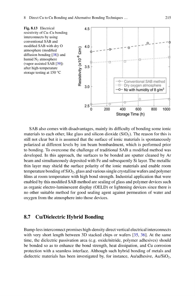
Fig. 8.13 Electrical
resistivity of Cu–Cu bonding
interconnects by using
conventional SAB and
modified SAB with dry O
atmosphere (modified
diffusion bonding [38]) and
humid N 2 atmosphere
(vapor-assisted SAB [39])
after high-temperature
storage testing at 150 °C
SAB also comes with disadvantages, mainly its difficulty of bonding some ionic
materials to each other, like glass and silicon dioxide (SiO 2 ). The reason for this is
still not clear but it is assumed that the surface of ionic materials is spontaneously
polarized at different levels by ion beam bombardment, which is performed prior
to bonding. To overcome the challenge of traditional SAB a modified method was
developed. In this approach, the surfaces to be bonded are sputter cleaned by Ar
beam and simultaneously deposited with Fe and subsequently Si layer. The metallic
thin layer may shield the surface polarity of the ionic materials and enable room
temperature bonding of SiO 2 , glass and various single crystalline wafers and polymer
films at room temperature with high bond strength. Industrial application that were
enabled by this modified SAB method are sealing of glass and polymer devices such
as organic electro-luminescent display (OELD) or lightening devices since there is
no other suitable method for good sealing agent against permeation of water and
oxygen from the atmosphere into those devices.
8.7 Cu/Dielectric Hybrid Bonding
Bump-less interconnect promises high-density direct vertical electrical interconnects
with very short length between 3D stacked chips or wafers [35, 36]. At the same
time, the dielectric passivation area (e.g. oxide/nitride, polymer adhesives) should
be bonded so as to enhance the bond strength, heat dissipation, and Cu corrosion
protection with a seamless interface. Although such hybrid bonding of metals and
dielectric materials has been investigated by, for instance, Au/adhesive, Au/SiO 2 ,
215
Fig. 8.13 Electrical
resistivity of Cu–Cu bonding
interconnects by using
conventional SAB and
modified SAB with dry O
atmosphere (modified
diffusion bonding [38]) and
humid N 2 atmosphere
(vapor-assisted SAB [39])
after high-temperature
storage testing at 150 °C
SAB also comes with disadvantages, mainly its difficulty of bonding some ionic
materials to each other, like glass and silicon dioxide (SiO 2 ). The reason for this is
still not clear but it is assumed that the surface of ionic materials is spontaneously
polarized at different levels by ion beam bombardment, which is performed prior
to bonding. To overcome the challenge of traditional SAB a modified method was
developed. In this approach, the surfaces to be bonded are sputter cleaned by Ar
beam and simultaneously deposited with Fe and subsequently Si layer. The metallic
thin layer may shield the surface polarity of the ionic materials and enable room
temperature bonding of SiO 2 , glass and various single crystalline wafers and polymer
films at room temperature with high bond strength. Industrial application that were
enabled by this modified SAB method are sealing of glass and polymer devices such
as organic electro-luminescent display (OELD) or lightening devices since there is
no other suitable method for good sealing agent against permeation of water and
oxygen from the atmosphere into those devices.
8.7 Cu/Dielectric Hybrid Bonding
Bump-less interconnect promises high-density direct vertical electrical interconnects
with very short length between 3D stacked chips or wafers [35, 36]. At the same
time, the dielectric passivation area (e.g. oxide/nitride, polymer adhesives) should
be bonded so as to enhance the bond strength, heat dissipation, and Cu corrosion
protection with a seamless interface. Although such hybrid bonding of metals and
dielectric materials has been investigated by, for instance, Au/adhesive, Au/SiO 2 ,