

8 Direct Cu to Cu Bonding and Alternative Bonding Techniques …
209
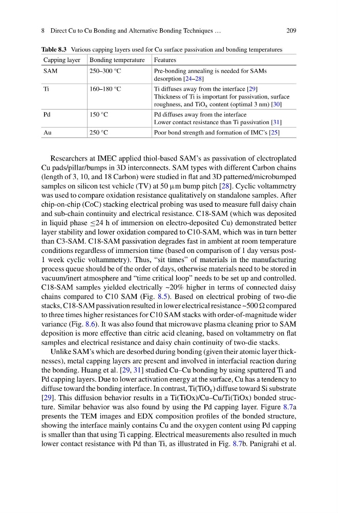
Table 8.3 Various capping layers used for Cu surface passivation and bonding temperatures
Capping layer Bonding temperature Features
SAM
250–300 °C
Pre-bonding annealing is needed for SAMs
desorption [24–28]
Ti
160–180 °C
Ti diffuses away from the interface [29]
Thickness of Ti is important for passivation, surface
roughness, and TiO x content (optimal 3 nm) [30]
Pd
150 °C
Pd diffuses away from the interface
Lower contact resistance than Ti passivation [31]
Au
250 °C
Poor bond strength and formation of IMC’s [25]
Researchers at IMEC applied thiol-based SAM’s as passivation of electroplated
Cu pads/pillar/bumps in 3D interconnects. SAM types with different Carbon chains
(length of 3, 10, and 18 Carbon) were studied in flat and 3D patterned/microbumped
samples on silicon test vehicle (TV) at 50 μm bump pitch [28]. Cyclic voltammetry
was used to compare oxidation resistance qualitatively on standalone samples. After
chip-on-chip (CoC) stacking electrical probing was used to measure full daisy chain
and sub-chain continuity and electrical resistance. C18-SAM (which was deposited
in liquid phase ≤24 h of immersion on electro-deposited Cu) demonstrated better
layer stability and lower oxidation compared to C10-SAM, which was in turn better
than C3-SAM. C18-SAM passivation degrades fast in ambient at room temperature
conditions regardless of immersion time (based on comparison of 1 day versus post1 week cyclic voltammetry). Thus, “sit times” of materials in the manufacturing
process queue should be of the order of days, otherwise materials need to be stored in
vacuum/inert atmosphere and “time critical loop” needs to be set up and controlled.
C18-SAM samples yielded electrically ~20% higher in terms of connected daisy
chains compared to C10 SAM (Fig. 8.5). Based on electrical probing of two-die
stacks, C18-SAM passivation resulted in lower electrical resistance ~500 compared
to three times higher resistances for C10 SAM stacks with order-of-magnitude wider
variance (Fig. 8.6). It was also found that microwave plasma cleaning prior to SAM
deposition is more effective than citric acid cleaning, based on voltammetry on flat
samples and electrical resistance and daisy chain continuity of two-die stacks.
Unlike SAM’s which are desorbed during bonding (given their atomic layer thicknesses), metal capping layers are present and involved in interfacial reaction during
the bonding. Huang et al. [29, 31] studied Cu–Cu bonding by using sputtered Ti and
Pd capping layers. Due to lower activation energy at the surface, Cu has a tendency to
diffuse toward the bonding interface. In contrast, Ti(TiO x ) diffuse toward Si substrate
[29]. This diffusion behavior results in a Ti(TiOx)/Cu–Cu/Ti(TiOx) bonded structure. Similar behavior was also found by using the Pd capping layer. Figure 8.7a
presents the TEM images and EDX composition profiles of the bonded structure,
showing the interface mainly contains Cu and the oxygen content using Pd capping
is smaller than that using Ti capping. Electrical measurements also resulted in much
lower contact resistance with Pd than Ti, as illustrated in Fig. 8.7b. Panigrahi et al.
209
Table 8.3 Various capping layers used for Cu surface passivation and bonding temperatures
Capping layer Bonding temperature Features
SAM
250–300 °C
Pre-bonding annealing is needed for SAMs
desorption [24–28]
Ti
160–180 °C
Ti diffuses away from the interface [29]
Thickness of Ti is important for passivation, surface
roughness, and TiO x content (optimal 3 nm) [30]
Pd
150 °C
Pd diffuses away from the interface
Lower contact resistance than Ti passivation [31]
Au
250 °C
Poor bond strength and formation of IMC’s [25]
Researchers at IMEC applied thiol-based SAM’s as passivation of electroplated
Cu pads/pillar/bumps in 3D interconnects. SAM types with different Carbon chains
(length of 3, 10, and 18 Carbon) were studied in flat and 3D patterned/microbumped
samples on silicon test vehicle (TV) at 50 μm bump pitch [28]. Cyclic voltammetry
was used to compare oxidation resistance qualitatively on standalone samples. After
chip-on-chip (CoC) stacking electrical probing was used to measure full daisy chain
and sub-chain continuity and electrical resistance. C18-SAM (which was deposited
in liquid phase ≤24 h of immersion on electro-deposited Cu) demonstrated better
layer stability and lower oxidation compared to C10-SAM, which was in turn better
than C3-SAM. C18-SAM passivation degrades fast in ambient at room temperature
conditions regardless of immersion time (based on comparison of 1 day versus post1 week cyclic voltammetry). Thus, “sit times” of materials in the manufacturing
process queue should be of the order of days, otherwise materials need to be stored in
vacuum/inert atmosphere and “time critical loop” needs to be set up and controlled.
C18-SAM samples yielded electrically ~20% higher in terms of connected daisy
chains compared to C10 SAM (Fig. 8.5). Based on electrical probing of two-die
stacks, C18-SAM passivation resulted in lower electrical resistance ~500 compared
to three times higher resistances for C10 SAM stacks with order-of-magnitude wider
variance (Fig. 8.6). It was also found that microwave plasma cleaning prior to SAM
deposition is more effective than citric acid cleaning, based on voltammetry on flat
samples and electrical resistance and daisy chain continuity of two-die stacks.
Unlike SAM’s which are desorbed during bonding (given their atomic layer thicknesses), metal capping layers are present and involved in interfacial reaction during
the bonding. Huang et al. [29, 31] studied Cu–Cu bonding by using sputtered Ti and
Pd capping layers. Due to lower activation energy at the surface, Cu has a tendency to
diffuse toward the bonding interface. In contrast, Ti(TiO x ) diffuse toward Si substrate
[29]. This diffusion behavior results in a Ti(TiOx)/Cu–Cu/Ti(TiOx) bonded structure. Similar behavior was also found by using the Pd capping layer. Figure 8.7a
presents the TEM images and EDX composition profiles of the bonded structure,
showing the interface mainly contains Cu and the oxygen content using Pd capping
is smaller than that using Ti capping. Electrical measurements also resulted in much
lower contact resistance with Pd than Ti, as illustrated in Fig. 8.7b. Panigrahi et al.