

1 Introduction to 3D Microelectronic Packaging
3
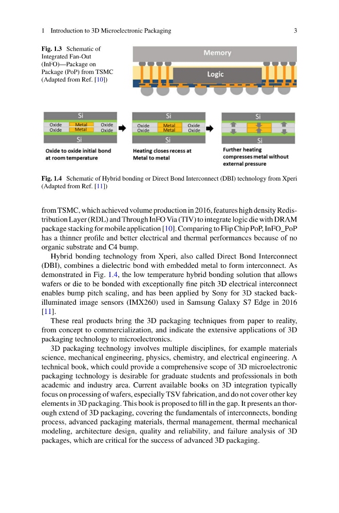
Fig. 1.3 Schematic of
Integrated Fan-Out
(InFO)—Package on
Package (PoP) from TSMC
(Adapted from Ref. [10])
Fig. 1.4 Schematic of Hybrid bonding or Direct Bond Interconnect (DBI) technology from Xperi
(Adapted from Ref. [11])
from TSMC, which achieved volume production in 2016, features high density Redistribution Layer (RDL) and Through InFO Via (TIV) to integrate logic die with DRAM
package stacking for mobile application [10]. Comparing to Flip Chip PoP, InFO_PoP
has a thinner profile and better electrical and thermal performances because of no
organic substrate and C4 bump.
Hybrid bonding technology from Xperi, also called Direct Bond Interconnect
(DBI), combines a dielectric bond with embedded metal to form interconnect. As
demonstrated in Fig. 1.4, the low temperature hybrid bonding solution that allows
wafers or die to be bonded with exceptionally fine pitch 3D electrical interconnect
enables bump pitch scaling, and has been applied by Sony for 3D stacked backilluminated image sensors (IMX260) used in Samsung Galaxy S7 Edge in 2016
[11].
These real products bring the 3D packaging techniques from paper to reality,
from concept to commercialization, and indicate the extensive applications of 3D
packaging technology to microelectronics.
3D packaging technology involves multiple disciplines, for example materials
science, mechanical engineering, physics, chemistry, and electrical engineering. A
technical book, which could provide a comprehensive scope of 3D microelectronic
packaging technology is desirable for graduate students and professionals in both
academic and industry area. Current available books on 3D integration typically
focus on processing of wafers, especially TSV fabrication, and do not cover other key
elements in 3D packaging. This book is proposed to fill in the gap. It presents an thorough extend of 3D packaging, covering the fundamentals of interconnects, bonding
process, advanced packaging materials, thermal management, thermal mechanical
modeling, architecture design, quality and reliability, and failure analysis of 3D
packages, which are critical for the success of advanced 3D packaging.
3
Fig. 1.3 Schematic of
Integrated Fan-Out
(InFO)—Package on
Package (PoP) from TSMC
(Adapted from Ref. [10])
Fig. 1.4 Schematic of Hybrid bonding or Direct Bond Interconnect (DBI) technology from Xperi
(Adapted from Ref. [11])
from TSMC, which achieved volume production in 2016, features high density Redistribution Layer (RDL) and Through InFO Via (TIV) to integrate logic die with DRAM
package stacking for mobile application [10]. Comparing to Flip Chip PoP, InFO_PoP
has a thinner profile and better electrical and thermal performances because of no
organic substrate and C4 bump.
Hybrid bonding technology from Xperi, also called Direct Bond Interconnect
(DBI), combines a dielectric bond with embedded metal to form interconnect. As
demonstrated in Fig. 1.4, the low temperature hybrid bonding solution that allows
wafers or die to be bonded with exceptionally fine pitch 3D electrical interconnect
enables bump pitch scaling, and has been applied by Sony for 3D stacked backilluminated image sensors (IMX260) used in Samsung Galaxy S7 Edge in 2016
[11].
These real products bring the 3D packaging techniques from paper to reality,
from concept to commercialization, and indicate the extensive applications of 3D
packaging technology to microelectronics.
3D packaging technology involves multiple disciplines, for example materials
science, mechanical engineering, physics, chemistry, and electrical engineering. A
technical book, which could provide a comprehensive scope of 3D microelectronic
packaging technology is desirable for graduate students and professionals in both
academic and industry area. Current available books on 3D integration typically
focus on processing of wafers, especially TSV fabrication, and do not cover other key
elements in 3D packaging. This book is proposed to fill in the gap. It presents an thorough extend of 3D packaging, covering the fundamentals of interconnects, bonding
process, advanced packaging materials, thermal management, thermal mechanical
modeling, architecture design, quality and reliability, and failure analysis of 3D
packages, which are critical for the success of advanced 3D packaging.