

2
Y. Li and D. Goyal
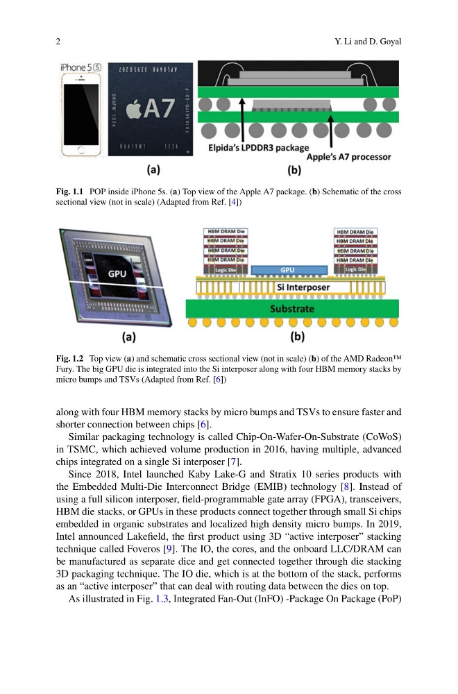
Fig. 1.1 POP inside iPhone 5s. (a) Top view of the Apple A7 package. (b) Schematic of the cross
sectional view (not in scale) (Adapted from Ref. [4])
Fig. 1.2 Top view (a) and schematic cross sectional view (not in scale) (b) of the AMD Radeon™
Fury. The big GPU die is integrated into the Si interposer along with four HBM memory stacks by
micro bumps and TSVs (Adapted from Ref. [6])
along with four HBM memory stacks by micro bumps and TSVs to ensure faster and
shorter connection between chips [6].
Similar packaging technology is called Chip-On-Wafer-On-Substrate (CoWoS)
in TSMC, which achieved volume production in 2016, having multiple, advanced
chips integrated on a single Si interposer [7].
Since 2018, Intel launched Kaby Lake-G and Stratix 10 series products with
the Embedded Multi-Die Interconnect Bridge (EMIB) technology [8]. Instead of
using a full silicon interposer, field-programmable gate array (FPGA), transceivers,
HBM die stacks, or GPUs in these products connect together through small Si chips
embedded in organic substrates and localized high density micro bumps. In 2019,
Intel announced Lakefield, the first product using 3D “active interposer” stacking
technique called Foveros [9]. The IO, the cores, and the onboard LLC/DRAM can
be manufactured as separate dice and get connected together through die stacking
3D packaging technique. The IO die, which is at the bottom of the stack, performs
as an “active interposer” that can deal with routing data between the dies on top.
As illustrated in Fig. 1.3, Integrated Fan-Out (InFO) -Package On Package (PoP)
Y. Li and D. Goyal
Fig. 1.1 POP inside iPhone 5s. (a) Top view of the Apple A7 package. (b) Schematic of the cross
sectional view (not in scale) (Adapted from Ref. [4])
Fig. 1.2 Top view (a) and schematic cross sectional view (not in scale) (b) of the AMD Radeon™
Fury. The big GPU die is integrated into the Si interposer along with four HBM memory stacks by
micro bumps and TSVs (Adapted from Ref. [6])
along with four HBM memory stacks by micro bumps and TSVs to ensure faster and
shorter connection between chips [6].
Similar packaging technology is called Chip-On-Wafer-On-Substrate (CoWoS)
in TSMC, which achieved volume production in 2016, having multiple, advanced
chips integrated on a single Si interposer [7].
Since 2018, Intel launched Kaby Lake-G and Stratix 10 series products with
the Embedded Multi-Die Interconnect Bridge (EMIB) technology [8]. Instead of
using a full silicon interposer, field-programmable gate array (FPGA), transceivers,
HBM die stacks, or GPUs in these products connect together through small Si chips
embedded in organic substrates and localized high density micro bumps. In 2019,
Intel announced Lakefield, the first product using 3D “active interposer” stacking
technique called Foveros [9]. The IO, the cores, and the onboard LLC/DRAM can
be manufactured as separate dice and get connected together through die stacking
3D packaging technique. The IO die, which is at the bottom of the stack, performs
as an “active interposer” that can deal with routing data between the dies on top.
As illustrated in Fig. 1.3, Integrated Fan-Out (InFO) -Package On Package (PoP)