

7 Fundamentals and Failures in Die Preparation for 3D Packaging
191
ramp rate depends on the laser wavelength, power and irradiation time as well as the
chip thickness and surrounding thermal resistances. For thick silicon, laser might be
completely absorbed by silicon; for thin silicon, laser might exit silicon after laser
absorption and enter chip BEOL. Once laser hits the metal lines inside chip BEOL,
part of laser will be reflected back into bulk silicon. So multiple reflection/absorption
might happen inside the chip. Once chip temperature reaches critical values, flux
activation, oxide removal, solder melting and wetting occur. Current state-of-art
LAB process uses IR camera to monitor the chip temperature. But this IR camera
temperature readings need to be calibrated by using actual chip and instrumenting
thermal couple between chip and substrate because emissivity is impacted by surface
roughness. For a good LAB process, the temperature curve measured by IR camera
should have a plateau region, which is related to phase change during solder melting.
During chip design, designer should pay attention to the bump array. If bump array
asymmetry is too big, chip tilt might occur during LAB process.
7.9 Underfill
Epoxy or underfill has been used for decades to fill the gap between chip and substrate
or between chip and chip. Some epoxies are pre-applied before chip attach and based
on squeezed flow while other epoxies are applied post chip attach and based on
capillary flow. The pros and cons for each type of epoxy have been discussed by
many groups in the past and won’t be repeated here [101].
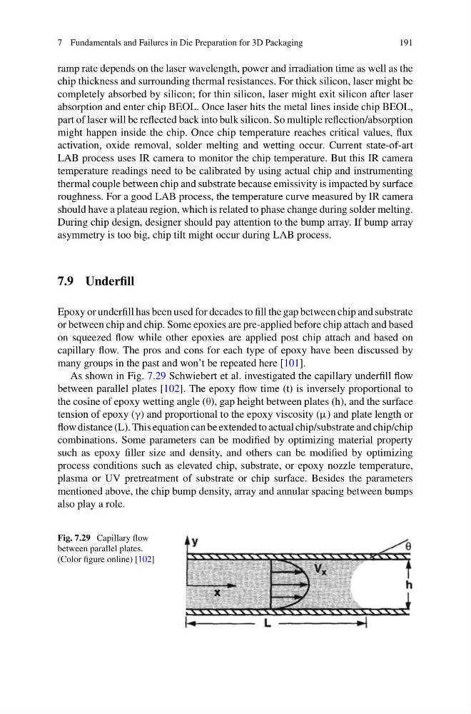
As shown in Fig. 7.29 Schwiebert et al. investigated the capillary underfill flow
between parallel plates [102]. The epoxy flow time (t) is inversely proportional to
the cosine of epoxy wetting angle (θ), gap height between plates (h), and the surface
tension of epoxy (γ) and proportional to the epoxy viscosity (μ) and plate length or
flow distance (L). This equation can be extended to actual chip/substrate and chip/chip
combinations. Some parameters can be modified by optimizing material property
such as epoxy filler size and density, and others can be modified by optimizing
process conditions such as elevated chip, substrate, or epoxy nozzle temperature,
plasma or UV pretreatment of substrate or chip surface. Besides the parameters
mentioned above, the chip bump density, array and annular spacing between bumps
also play a role.
Fig. 7.29 Capillary flow
between parallel plates.
(Color figure online) [102]
191
ramp rate depends on the laser wavelength, power and irradiation time as well as the
chip thickness and surrounding thermal resistances. For thick silicon, laser might be
completely absorbed by silicon; for thin silicon, laser might exit silicon after laser
absorption and enter chip BEOL. Once laser hits the metal lines inside chip BEOL,
part of laser will be reflected back into bulk silicon. So multiple reflection/absorption
might happen inside the chip. Once chip temperature reaches critical values, flux
activation, oxide removal, solder melting and wetting occur. Current state-of-art
LAB process uses IR camera to monitor the chip temperature. But this IR camera
temperature readings need to be calibrated by using actual chip and instrumenting
thermal couple between chip and substrate because emissivity is impacted by surface
roughness. For a good LAB process, the temperature curve measured by IR camera
should have a plateau region, which is related to phase change during solder melting.
During chip design, designer should pay attention to the bump array. If bump array
asymmetry is too big, chip tilt might occur during LAB process.
7.9 Underfill
Epoxy or underfill has been used for decades to fill the gap between chip and substrate
or between chip and chip. Some epoxies are pre-applied before chip attach and based
on squeezed flow while other epoxies are applied post chip attach and based on
capillary flow. The pros and cons for each type of epoxy have been discussed by
many groups in the past and won’t be repeated here [101].
As shown in Fig. 7.29 Schwiebert et al. investigated the capillary underfill flow
between parallel plates [102]. The epoxy flow time (t) is inversely proportional to
the cosine of epoxy wetting angle (θ), gap height between plates (h), and the surface
tension of epoxy (γ) and proportional to the epoxy viscosity (μ) and plate length or
flow distance (L). This equation can be extended to actual chip/substrate and chip/chip
combinations. Some parameters can be modified by optimizing material property
such as epoxy filler size and density, and others can be modified by optimizing
process conditions such as elevated chip, substrate, or epoxy nozzle temperature,
plasma or UV pretreatment of substrate or chip surface. Besides the parameters
mentioned above, the chip bump density, array and annular spacing between bumps
also play a role.
Fig. 7.29 Capillary flow
between parallel plates.
(Color figure online) [102]