

190
H. Ma et al.
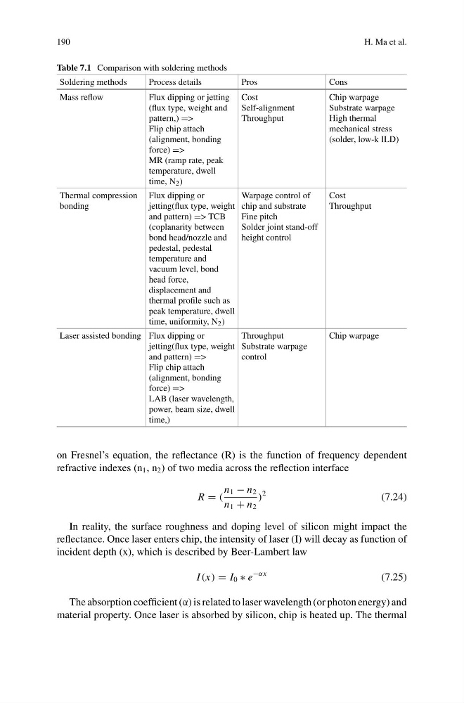
Table 7.1 Comparison with soldering methods
Soldering methods
Process details
Pros
Cons
Mass reflow
Flux dipping or jetting
(flux type, weight and
pattern,) =>
Flip chip attach
(alignment, bonding
force) =>
MR (ramp rate, peak
temperature, dwell
time, N 2 )
Cost
Self-alignment
Throughput
Chip warpage
Substrate warpage
High thermal
mechanical stress
(solder, low-k ILD)
Thermal compression
bonding
Flux dipping or
jetting(flux type, weight
and pattern) => TCB
(coplanarity between
bond head/nozzle and
pedestal, pedestal
temperature and
vacuum level, bond
head force,
displacement and
thermal profile such as
peak temperature, dwell
time, uniformity, N 2 )
Warpage control of
chip and substrate
Fine pitch
Solder joint stand-off
height control
Cost
Throughput
Laser assisted bonding Flux dipping or
jetting(flux type, weight
and pattern) =>
Flip chip attach
(alignment, bonding
force) =>
LAB (laser wavelength,
power, beam size, dwell
time,)
Throughput
Substrate warpage
control
Chip warpage
on Fresnel’s equation, the reflectance (R) is the function of frequency dependent
refractive indexes (n 1 , n 2 ) of two media across the reflection interface
R = (
n 1 − n 2
n 1 + n 2
)
2
(7.24)
In reality, the surface roughness and doping level of silicon might impact the
reflectance. Once laser enters chip, the intensity of laser (I) will decay as function of
incident depth (x), which is described by Beer-Lambert law
I (x) = I 0 ∗ e
−αx
(7.25)
The absorption coefficient (α) is related to laser wavelength (or photon energy) and
material property. Once laser is absorbed by silicon, chip is heated up. The thermal
H. Ma et al.
Table 7.1 Comparison with soldering methods
Soldering methods
Process details
Pros
Cons
Mass reflow
Flux dipping or jetting
(flux type, weight and
pattern,) =>
Flip chip attach
(alignment, bonding
force) =>
MR (ramp rate, peak
temperature, dwell
time, N 2 )
Cost
Self-alignment
Throughput
Chip warpage
Substrate warpage
High thermal
mechanical stress
(solder, low-k ILD)
Thermal compression
bonding
Flux dipping or
jetting(flux type, weight
and pattern) => TCB
(coplanarity between
bond head/nozzle and
pedestal, pedestal
temperature and
vacuum level, bond
head force,
displacement and
thermal profile such as
peak temperature, dwell
time, uniformity, N 2 )
Warpage control of
chip and substrate
Fine pitch
Solder joint stand-off
height control
Cost
Throughput
Laser assisted bonding Flux dipping or
jetting(flux type, weight
and pattern) =>
Flip chip attach
(alignment, bonding
force) =>
LAB (laser wavelength,
power, beam size, dwell
time,)
Throughput
Substrate warpage
control
Chip warpage
on Fresnel’s equation, the reflectance (R) is the function of frequency dependent
refractive indexes (n 1 , n 2 ) of two media across the reflection interface
R = (
n 1 − n 2
n 1 + n 2
)
2
(7.24)
In reality, the surface roughness and doping level of silicon might impact the
reflectance. Once laser enters chip, the intensity of laser (I) will decay as function of
incident depth (x), which is described by Beer-Lambert law
I (x) = I 0 ∗ e
−αx
(7.25)
The absorption coefficient (α) is related to laser wavelength (or photon energy) and
material property. Once laser is absorbed by silicon, chip is heated up. The thermal