

7 Fundamentals and Failures in Die Preparation for 3D Packaging
179
reliability and cost demand. The immediate potential applications of laser include
laser dicing for thin wafer, and laser scribe or grooving for wafer with complex or
challenging ILD stack before mechanical saw dicing.
The key and fundamental advantages of laser process include [64]:
1. Laser cuts smaller street width due to narrow beam diameter and hence can enable
narrow street width which can increase number of chips per wafer.
2. Laser singulation can enable non-Cartesian street. This can enable multi chip
size vehicle and harvest various chip sizes from same wafer.
3. Laser through cut for thin wafer reduces or eliminates die edge defects and cracks.
4. Laser dicing or scribe is a “dry” process in contrast with saw process and hence
potentially eliminates any corrosion and moisture related issue. This advantage
may be limited due to wafer coat requirement and post laser singulation wash.
However, the time used is significantly less compared to that during saw process.
Multiple publications reported that although saw technology continue to
progress in semiconductor dicing, there are challenges and difficulty in meeting
yield/reliability requirement when the die thickness are reduced below 100 um [63–
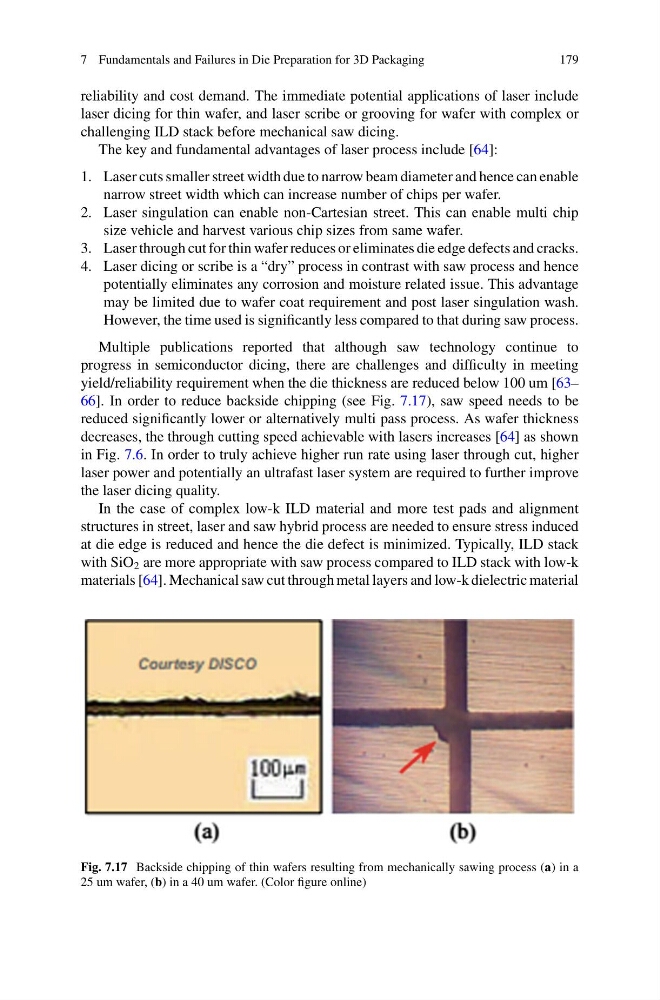
66]. In order to reduce backside chipping (see Fig. 7.17), saw speed needs to be
reduced significantly lower or alternatively multi pass process. As wafer thickness
decreases, the through cutting speed achievable with lasers increases [64] as shown
in Fig. 7.6. In order to truly achieve higher run rate using laser through cut, higher
laser power and potentially an ultrafast laser system are required to further improve
the laser dicing quality.
In the case of complex low-k ILD material and more test pads and alignment
structures in street, laser and saw hybrid process are needed to ensure stress induced
at die edge is reduced and hence the die defect is minimized. Typically, ILD stack
with SiO 2 are more appropriate with saw process compared to ILD stack with low-k
materials [64]. Mechanical saw cut through metal layers and low-k dielectric material
Fig. 7.17 Backside chipping of thin wafers resulting from mechanically sawing process (a) in a
25 um wafer, (b) in a 40 um wafer. (Color figure online)
179
reliability and cost demand. The immediate potential applications of laser include
laser dicing for thin wafer, and laser scribe or grooving for wafer with complex or
challenging ILD stack before mechanical saw dicing.
The key and fundamental advantages of laser process include [64]:
1. Laser cuts smaller street width due to narrow beam diameter and hence can enable
narrow street width which can increase number of chips per wafer.
2. Laser singulation can enable non-Cartesian street. This can enable multi chip
size vehicle and harvest various chip sizes from same wafer.
3. Laser through cut for thin wafer reduces or eliminates die edge defects and cracks.
4. Laser dicing or scribe is a “dry” process in contrast with saw process and hence
potentially eliminates any corrosion and moisture related issue. This advantage
may be limited due to wafer coat requirement and post laser singulation wash.
However, the time used is significantly less compared to that during saw process.
Multiple publications reported that although saw technology continue to
progress in semiconductor dicing, there are challenges and difficulty in meeting
yield/reliability requirement when the die thickness are reduced below 100 um [63–
66]. In order to reduce backside chipping (see Fig. 7.17), saw speed needs to be
reduced significantly lower or alternatively multi pass process. As wafer thickness
decreases, the through cutting speed achievable with lasers increases [64] as shown
in Fig. 7.6. In order to truly achieve higher run rate using laser through cut, higher
laser power and potentially an ultrafast laser system are required to further improve
the laser dicing quality.
In the case of complex low-k ILD material and more test pads and alignment
structures in street, laser and saw hybrid process are needed to ensure stress induced
at die edge is reduced and hence the die defect is minimized. Typically, ILD stack
with SiO 2 are more appropriate with saw process compared to ILD stack with low-k
materials [64]. Mechanical saw cut through metal layers and low-k dielectric material
Fig. 7.17 Backside chipping of thin wafers resulting from mechanically sawing process (a) in a
25 um wafer, (b) in a 40 um wafer. (Color figure online)