

178
H. Ma et al.
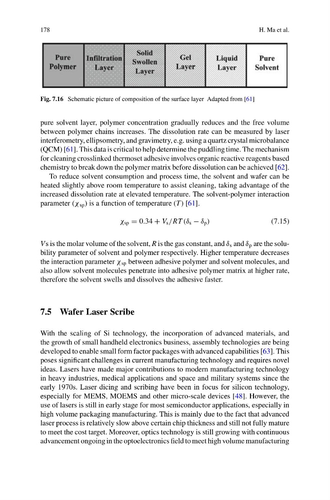
Fig. 7.16 Schematic picture of composition of the surface layer Adapted from [61]
pure solvent layer, polymer concentration gradually reduces and the free volume
between polymer chains increases. The dissolution rate can be measured by laser
interferometry, ellipsometry, and gravimetry, e.g. using a quartz crystal microbalance
(QCM) [61]. This data is critical to help determine the puddling time. The mechanism
for cleaning crosslinked thermoset adhesive involves organic reactive reagents based
chemistry to break down the polymer matrix before dissolution can be achieved [62].
To reduce solvent consumption and process time, the solvent and wafer can be
heated slightly above room temperature to assist cleaning, taking advantage of the
increased dissolution rate at elevated temperature. The solvent-polymer interaction
parameter (χ sp ) is a function of temperature (T ) [61].
χ sp = 0.34 + V s /RT (δ s − δ p )
(7.15)
V s is the molar volume of the solvent, R is the gas constant, and δ s and δ p are the solubility parameter of solvent and polymer respectively. Higher temperature decreases
the interaction parameter χ sp between adhesive polymer and solvent molecules, and
also allow solvent molecules penetrate into adhesive polymer matrix at higher rate,
therefore the solvent swells and dissolves the adhesive faster.
7.5 Wafer Laser Scribe
With the scaling of Si technology, the incorporation of advanced materials, and
the growth of small handheld electronics business, assembly technologies are being
developed to enable small form factor packages with advanced capabilities [63]. This
poses significant challenges in current manufacturing technology and requires novel
ideas. Lasers have made major contributions to modern manufacturing technology
in heavy industries, medical applications and space and military systems since the
early 1970s. Laser dicing and scribing have been in focus for silicon technology,
especially for MEMS, MOEMS and other micro-scale devices [48]. However, the
use of lasers is still in early stage for most semiconductor applications, especially in
high volume packaging manufacturing. This is mainly due to the fact that advanced
laser process is relatively slow above certain chip thickness and still not fully mature
to meet the cost target. Moreover, optics technology is still growing with continuous
advancement ongoing in the optoelectronics field to meet high volume manufacturing
H. Ma et al.
Fig. 7.16 Schematic picture of composition of the surface layer Adapted from [61]
pure solvent layer, polymer concentration gradually reduces and the free volume
between polymer chains increases. The dissolution rate can be measured by laser
interferometry, ellipsometry, and gravimetry, e.g. using a quartz crystal microbalance
(QCM) [61]. This data is critical to help determine the puddling time. The mechanism
for cleaning crosslinked thermoset adhesive involves organic reactive reagents based
chemistry to break down the polymer matrix before dissolution can be achieved [62].
To reduce solvent consumption and process time, the solvent and wafer can be
heated slightly above room temperature to assist cleaning, taking advantage of the
increased dissolution rate at elevated temperature. The solvent-polymer interaction
parameter (χ sp ) is a function of temperature (T ) [61].
χ sp = 0.34 + V s /RT (δ s − δ p )
(7.15)
V s is the molar volume of the solvent, R is the gas constant, and δ s and δ p are the solubility parameter of solvent and polymer respectively. Higher temperature decreases
the interaction parameter χ sp between adhesive polymer and solvent molecules, and
also allow solvent molecules penetrate into adhesive polymer matrix at higher rate,
therefore the solvent swells and dissolves the adhesive faster.
7.5 Wafer Laser Scribe
With the scaling of Si technology, the incorporation of advanced materials, and
the growth of small handheld electronics business, assembly technologies are being
developed to enable small form factor packages with advanced capabilities [63]. This
poses significant challenges in current manufacturing technology and requires novel
ideas. Lasers have made major contributions to modern manufacturing technology
in heavy industries, medical applications and space and military systems since the
early 1970s. Laser dicing and scribing have been in focus for silicon technology,
especially for MEMS, MOEMS and other micro-scale devices [48]. However, the
use of lasers is still in early stage for most semiconductor applications, especially in
high volume packaging manufacturing. This is mainly due to the fact that advanced
laser process is relatively slow above certain chip thickness and still not fully mature
to meet the cost target. Moreover, optics technology is still growing with continuous
advancement ongoing in the optoelectronics field to meet high volume manufacturing