

180
H. Ma et al.
causes high chipping due to blade loading and hence higher blade bending which
can lead to die edge defects. A key solution for this issue is using laser scribe process
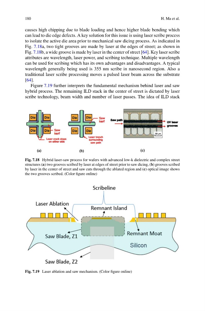
to isolate the active die area prior to mechanical saw dicing process. As indicated in
Fig. 7.18a, two tight grooves are made by laser at the edges of street; as shown in
Fig. 7.18b, a wide groove is made by laser in the center of street [64]. Key laser scribe
attributes are wavelength, laser power, and scribing technique. Multiple wavelength
can be used for scribing which has its own advantages and disadvantages. A typical
wavelength generally being used is 355 nm scribe in nanosecond region. Also a
traditional laser scribe processing moves a pulsed laser beam across the substrate
[64].
Figure 7.19 further interprets the fundamental mechanism behind laser and saw
hybrid process. The remaining ILD stack in the center of street is dictated by laser
scribe technology, beam width and number of laser passes. The idea of ILD stack
Fig. 7.18 Hybrid laser-saw process for wafers with advanced low-k dielectric and complex street
structures (a) two grooves scribed by laser at edges of street prior to saw dicing, (b) grooves scribed
by laser in the center of street and saw cuts through the ablated region and (c) optical image shows
the two grooves scribed. (Color figure online)
Fig. 7.19 Laser ablation and saw mechanism. (Color figure online)
H. Ma et al.
causes high chipping due to blade loading and hence higher blade bending which
can lead to die edge defects. A key solution for this issue is using laser scribe process
to isolate the active die area prior to mechanical saw dicing process. As indicated in
Fig. 7.18a, two tight grooves are made by laser at the edges of street; as shown in
Fig. 7.18b, a wide groove is made by laser in the center of street [64]. Key laser scribe
attributes are wavelength, laser power, and scribing technique. Multiple wavelength
can be used for scribing which has its own advantages and disadvantages. A typical
wavelength generally being used is 355 nm scribe in nanosecond region. Also a
traditional laser scribe processing moves a pulsed laser beam across the substrate
[64].
Figure 7.19 further interprets the fundamental mechanism behind laser and saw
hybrid process. The remaining ILD stack in the center of street is dictated by laser
scribe technology, beam width and number of laser passes. The idea of ILD stack
Fig. 7.18 Hybrid laser-saw process for wafers with advanced low-k dielectric and complex street
structures (a) two grooves scribed by laser at edges of street prior to saw dicing, (b) grooves scribed
by laser in the center of street and saw cuts through the ablated region and (c) optical image shows
the two grooves scribed. (Color figure online)
Fig. 7.19 Laser ablation and saw mechanism. (Color figure online)