

174
H. Ma et al.
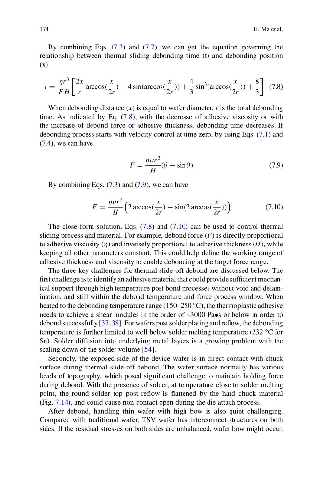
By combining Eqs. (7.3) and (7.7), we can get the equation governing the
relationship between thermal sliding debonding time (t) and debonding position
(x)
t =
ηr
3
F H
2x
r
arccos(
x
2r
) − 4 sin(arccos(
x
2r
)) +
4
3
sin
3
(arccos(
x
2r
)) +
8
3
(7.8)
When debonding distance (x) is equal to wafer diameter, t is the total debonding
time. As indicated by Eq. (7.8), with the decrease of adhesive viscosity or with
the increase of debond force or adhesive thickness, debonding time decreases. If
debonding process starts with velocity control at time zero, by using Eqs. (7.1) and
(7.4), we can have
F =
ηυr
2
H
(θ − sin θ)
(7.9)
By combining Eqs. (7.3) and (7.9), we can have
F =
ηυr
2
H
2 arccos(
x
2r
) − sin(2 arccos(
x
2r
))
(7.10)
The close-form solution, Eqs. (7.8) and (7.10) can be used to control thermal
sliding process and material. For example, debond force (F) is directly proportional
to adhesive viscosity (η) and inversely proportional to adhesive thickness (H), while
keeping all other parameters constant. This could help define the working range of
adhesive thickness and viscosity to enable debonding at the target force range.
The three key challenges for thermal slide-off debond are discussed below. The
first challenge is to identify an adhesive material that could provide sufficient mechanical support through high temperature post bond processes without void and delamination, and still within the debond temperature and force process window. When
heated to the debonding temperature range (150–250 °C), the thermoplastic adhesive
needs to achieve a shear modules in the order of ~3000 Pa•s or below in order to
debond successfully [37, 38]. For wafers post solder plating and reflow, the debonding
temperature is further limited to well below solder melting temperature (232 °C for
Sn). Solder diffusion into underlying metal layers is a growing problem with the
scaling down of the solder volume [54].
Secondly, the exposed side of the device wafer is in direct contact with chuck
surface during thermal slide-off debond. The wafer surface normally has various
levels of topography, which posed significant challenge to maintain holding force
during debond. With the presence of solder, at temperature close to solder melting
point, the round solder top post reflow is flattened by the hard chuck material
(Fig. 7.14), and could cause non-contact open during the die attach process.
After debond, handling thin wafer with high bow is also quiet challenging.
Compared with traditional wafer, TSV wafer has interconnect structures on both
sides. If the residual stresses on both sides are unbalanced, wafer bow might occur.
H. Ma et al.
By combining Eqs. (7.3) and (7.7), we can get the equation governing the
relationship between thermal sliding debonding time (t) and debonding position
(x)
t =
ηr
3
F H
2x
r
arccos(
x
2r
) − 4 sin(arccos(
x
2r
)) +
4
3
sin
3
(arccos(
x
2r
)) +
8
3
(7.8)
When debonding distance (x) is equal to wafer diameter, t is the total debonding
time. As indicated by Eq. (7.8), with the decrease of adhesive viscosity or with
the increase of debond force or adhesive thickness, debonding time decreases. If
debonding process starts with velocity control at time zero, by using Eqs. (7.1) and
(7.4), we can have
F =
ηυr
2
H
(θ − sin θ)
(7.9)
By combining Eqs. (7.3) and (7.9), we can have
F =
ηυr
2
H
2 arccos(
x
2r
) − sin(2 arccos(
x
2r
))
(7.10)
The close-form solution, Eqs. (7.8) and (7.10) can be used to control thermal
sliding process and material. For example, debond force (F) is directly proportional
to adhesive viscosity (η) and inversely proportional to adhesive thickness (H), while
keeping all other parameters constant. This could help define the working range of
adhesive thickness and viscosity to enable debonding at the target force range.
The three key challenges for thermal slide-off debond are discussed below. The
first challenge is to identify an adhesive material that could provide sufficient mechanical support through high temperature post bond processes without void and delamination, and still within the debond temperature and force process window. When
heated to the debonding temperature range (150–250 °C), the thermoplastic adhesive
needs to achieve a shear modules in the order of ~3000 Pa•s or below in order to
debond successfully [37, 38]. For wafers post solder plating and reflow, the debonding
temperature is further limited to well below solder melting temperature (232 °C for
Sn). Solder diffusion into underlying metal layers is a growing problem with the
scaling down of the solder volume [54].
Secondly, the exposed side of the device wafer is in direct contact with chuck
surface during thermal slide-off debond. The wafer surface normally has various
levels of topography, which posed significant challenge to maintain holding force
during debond. With the presence of solder, at temperature close to solder melting
point, the round solder top post reflow is flattened by the hard chuck material
(Fig. 7.14), and could cause non-contact open during the die attach process.
After debond, handling thin wafer with high bow is also quiet challenging.
Compared with traditional wafer, TSV wafer has interconnect structures on both
sides. If the residual stresses on both sides are unbalanced, wafer bow might occur.