

7 Fundamentals and Failures in Die Preparation for 3D Packaging
175
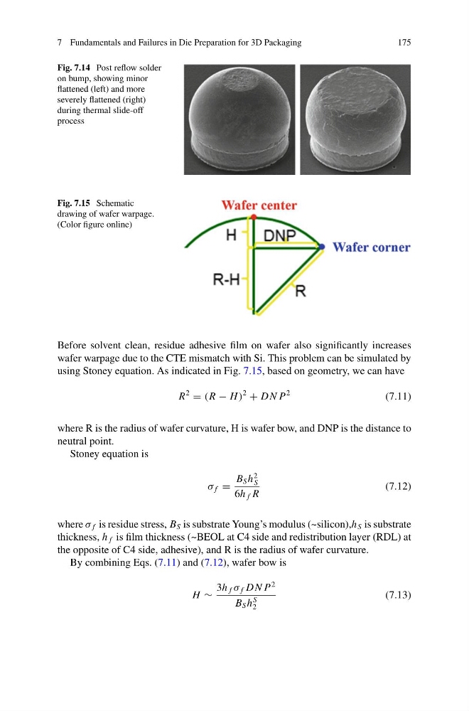
Fig. 7.14 Post reflow solder
on bump, showing minor
flattened (left) and more
severely flattened (right)
during thermal slide-off
process
Fig. 7.15 Schematic
drawing of wafer warpage.
(Color figure online)
Before solvent clean, residue adhesive film on wafer also significantly increases
wafer warpage due to the CTE mismatch with Si. This problem can be simulated by
using Stoney equation. As indicated in Fig. 7.15, based on geometry, we can have
R
2
= (R − H )
2
+ DN P
2
(7.11)
where R is the radius of wafer curvature, H is wafer bow, and DNP is the distance to
neutral point.
Stoney equation is
σ f =
B S h
2
S
6h f R
(7.12)
where σ f is residue stress, B S is substrate Young’s modulus (~silicon),h S is substrate
thickness, h f is film thickness (~BEOL at C4 side and redistribution layer (RDL) at
the opposite of C4 side, adhesive), and R is the radius of wafer curvature.
By combining Eqs. (7.11) and (7.12), wafer bow is
H ∼
3h f σ f DN P
2
B S h
S
2
(7.13)
175
Fig. 7.14 Post reflow solder
on bump, showing minor
flattened (left) and more
severely flattened (right)
during thermal slide-off
process
Fig. 7.15 Schematic
drawing of wafer warpage.
(Color figure online)
Before solvent clean, residue adhesive film on wafer also significantly increases
wafer warpage due to the CTE mismatch with Si. This problem can be simulated by
using Stoney equation. As indicated in Fig. 7.15, based on geometry, we can have
R
2
= (R − H )
2
+ DN P
2
(7.11)
where R is the radius of wafer curvature, H is wafer bow, and DNP is the distance to
neutral point.
Stoney equation is
σ f =
B S h
2
S
6h f R
(7.12)
where σ f is residue stress, B S is substrate Young’s modulus (~silicon),h S is substrate
thickness, h f is film thickness (~BEOL at C4 side and redistribution layer (RDL) at
the opposite of C4 side, adhesive), and R is the radius of wafer curvature.
By combining Eqs. (7.11) and (7.12), wafer bow is
H ∼
3h f σ f DN P
2
B S h
S
2
(7.13)