

162
H. Ma et al.
Si
Cu
Barrier
Dielectric liner
Depletion zone
w
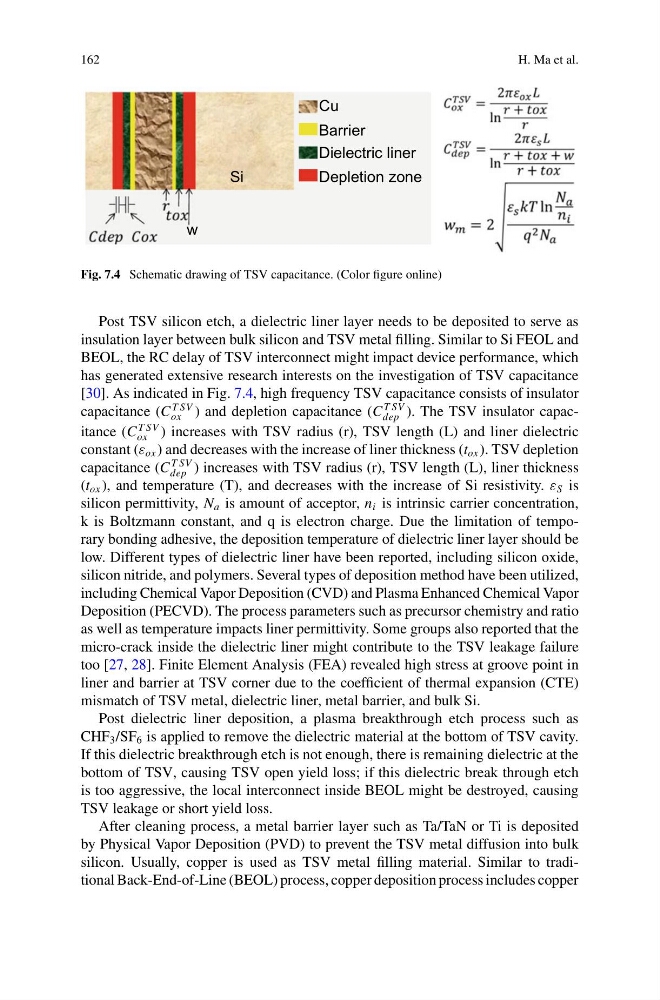
Fig. 7.4 Schematic drawing of TSV capacitance. (Color figure online)
Post TSV silicon etch, a dielectric liner layer needs to be deposited to serve as
insulation layer between bulk silicon and TSV metal filling. Similar to Si FEOL and
BEOL, the RC delay of TSV interconnect might impact device performance, which
has generated extensive research interests on the investigation of TSV capacitance
[30]. As indicated in Fig. 7.4, high frequency TSV capacitance consists of insulator
capacitance (C
T SV
ox ) and depletion capacitance (C
T SV
dep ). The TSV insulator capacitance (C
T SV
ox ) increases with TSV radius (r), TSV length (L) and liner dielectric
constant (ε ox ) and decreases with the increase of liner thickness (t ox ). TSV depletion
capacitance (C
T SV
dep ) increases with TSV radius (r), TSV length (L), liner thickness
(t ox ), and temperature (T), and decreases with the increase of Si resistivity. ε S is
silicon permittivity, N a is amount of acceptor, n i is intrinsic carrier concentration,
k is Boltzmann constant, and q is electron charge. Due the limitation of temporary bonding adhesive, the deposition temperature of dielectric liner layer should be
low. Different types of dielectric liner have been reported, including silicon oxide,
silicon nitride, and polymers. Several types of deposition method have been utilized,
including Chemical Vapor Deposition (CVD) and Plasma Enhanced Chemical Vapor
Deposition (PECVD). The process parameters such as precursor chemistry and ratio
as well as temperature impacts liner permittivity. Some groups also reported that the
micro-crack inside the dielectric liner might contribute to the TSV leakage failure
too [27, 28]. Finite Element Analysis (FEA) revealed high stress at groove point in
liner and barrier at TSV corner due to the coefficient of thermal expansion (CTE)
mismatch of TSV metal, dielectric liner, metal barrier, and bulk Si.
Post dielectric liner deposition, a plasma breakthrough etch process such as
CHF 3 /SF 6 is applied to remove the dielectric material at the bottom of TSV cavity.
If this dielectric breakthrough etch is not enough, there is remaining dielectric at the
bottom of TSV, causing TSV open yield loss; if this dielectric break through etch
is too aggressive, the local interconnect inside BEOL might be destroyed, causing
TSV leakage or short yield loss.
After cleaning process, a metal barrier layer such as Ta/TaN or Ti is deposited
by Physical Vapor Deposition (PVD) to prevent the TSV metal diffusion into bulk
silicon. Usually, copper is used as TSV metal filling material. Similar to traditional Back-End-of-Line (BEOL) process, copper deposition process includes copper
H. Ma et al.
Si
Cu
Barrier
Dielectric liner
Depletion zone
w
Fig. 7.4 Schematic drawing of TSV capacitance. (Color figure online)
Post TSV silicon etch, a dielectric liner layer needs to be deposited to serve as
insulation layer between bulk silicon and TSV metal filling. Similar to Si FEOL and
BEOL, the RC delay of TSV interconnect might impact device performance, which
has generated extensive research interests on the investigation of TSV capacitance
[30]. As indicated in Fig. 7.4, high frequency TSV capacitance consists of insulator
capacitance (C
T SV
ox ) and depletion capacitance (C
T SV
dep ). The TSV insulator capacitance (C
T SV
ox ) increases with TSV radius (r), TSV length (L) and liner dielectric
constant (ε ox ) and decreases with the increase of liner thickness (t ox ). TSV depletion
capacitance (C
T SV
dep ) increases with TSV radius (r), TSV length (L), liner thickness
(t ox ), and temperature (T), and decreases with the increase of Si resistivity. ε S is
silicon permittivity, N a is amount of acceptor, n i is intrinsic carrier concentration,
k is Boltzmann constant, and q is electron charge. Due the limitation of temporary bonding adhesive, the deposition temperature of dielectric liner layer should be
low. Different types of dielectric liner have been reported, including silicon oxide,
silicon nitride, and polymers. Several types of deposition method have been utilized,
including Chemical Vapor Deposition (CVD) and Plasma Enhanced Chemical Vapor
Deposition (PECVD). The process parameters such as precursor chemistry and ratio
as well as temperature impacts liner permittivity. Some groups also reported that the
micro-crack inside the dielectric liner might contribute to the TSV leakage failure
too [27, 28]. Finite Element Analysis (FEA) revealed high stress at groove point in
liner and barrier at TSV corner due to the coefficient of thermal expansion (CTE)
mismatch of TSV metal, dielectric liner, metal barrier, and bulk Si.
Post dielectric liner deposition, a plasma breakthrough etch process such as
CHF 3 /SF 6 is applied to remove the dielectric material at the bottom of TSV cavity.
If this dielectric breakthrough etch is not enough, there is remaining dielectric at the
bottom of TSV, causing TSV open yield loss; if this dielectric break through etch
is too aggressive, the local interconnect inside BEOL might be destroyed, causing
TSV leakage or short yield loss.
After cleaning process, a metal barrier layer such as Ta/TaN or Ti is deposited
by Physical Vapor Deposition (PVD) to prevent the TSV metal diffusion into bulk
silicon. Usually, copper is used as TSV metal filling material. Similar to traditional Back-End-of-Line (BEOL) process, copper deposition process includes copper