

94
P. Kumar et al.
Fig. 4.24 (a) Chip showing a TSV with metal lines at top and bottom. Voids form due to EM at
300 °C at exits of electron flow at top and bottom for thin metal-lines (b) and (c) and thick metal
lines (d) and (e) [62]
not susceptible to EM damage, the BEOL and RDL structures in the device can be
significantly affected by EM.
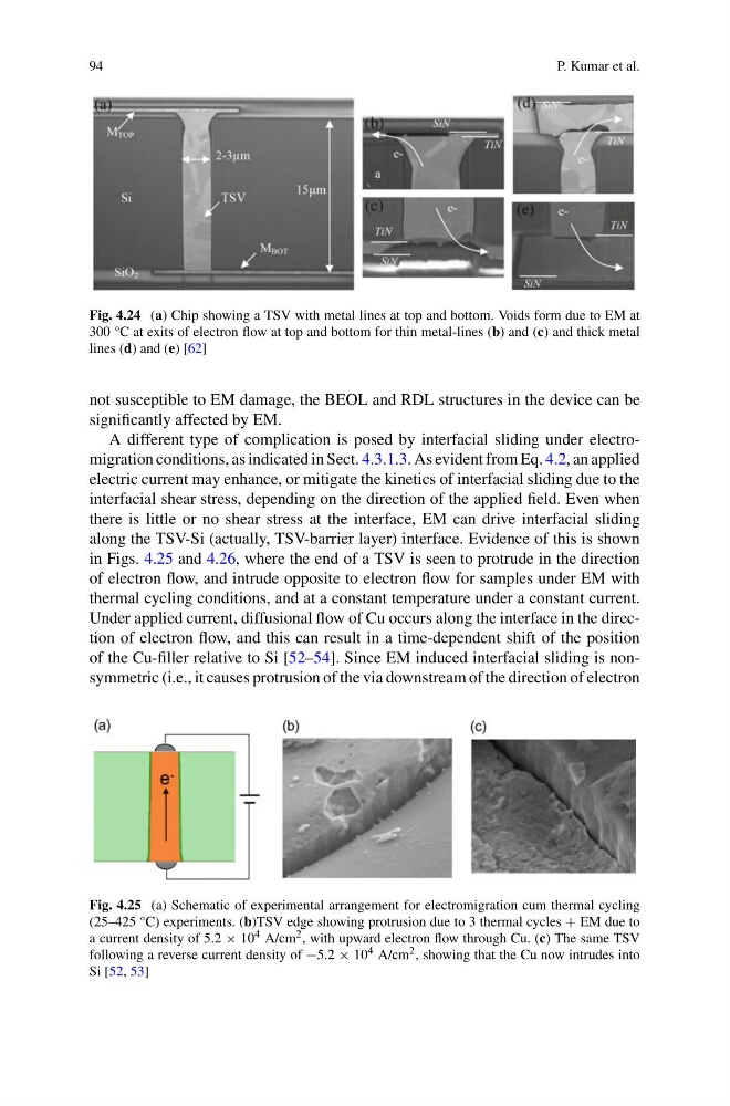
A different type of complication is posed by interfacial sliding under electromigration conditions, as indicated in Sect. 4.3.1.3. As evident from Eq. 4.2, an applied
electric current may enhance, or mitigate the kinetics of interfacial sliding due to the
interfacial shear stress, depending on the direction of the applied field. Even when
there is little or no shear stress at the interface, EM can drive interfacial sliding
along the TSV-Si (actually, TSV-barrier layer) interface. Evidence of this is shown
in Figs. 4.25 and 4.26, where the end of a TSV is seen to protrude in the direction
of electron flow, and intrude opposite to electron flow for samples under EM with
thermal cycling conditions, and at a constant temperature under a constant current.
Under applied current, diffusional flow of Cu occurs along the interface in the direction of electron flow, and this can result in a time-dependent shift of the position
of the Cu-filler relative to Si [52–54]. Since EM induced interfacial sliding is nonsymmetric (i.e., it causes protrusion of the via downstream of the direction of electron
Fig. 4.25 (a) Schematic of experimental arrangement for electromigration cum thermal cycling
(25–425 °C) experiments. (b)TSV edge showing protrusion due to 3 thermal cycles + EM due to
a current density of 5.2 × 10 4 A/cm 2 , with upward electron flow through Cu. (c) The same TSV
following a reverse current density of −5.2 × 10 4 A/cm 2 , showing that the Cu now intrudes into
Si [52, 53]
P. Kumar et al.
Fig. 4.24 (a) Chip showing a TSV with metal lines at top and bottom. Voids form due to EM at
300 °C at exits of electron flow at top and bottom for thin metal-lines (b) and (c) and thick metal
lines (d) and (e) [62]
not susceptible to EM damage, the BEOL and RDL structures in the device can be
significantly affected by EM.
A different type of complication is posed by interfacial sliding under electromigration conditions, as indicated in Sect. 4.3.1.3. As evident from Eq. 4.2, an applied
electric current may enhance, or mitigate the kinetics of interfacial sliding due to the
interfacial shear stress, depending on the direction of the applied field. Even when
there is little or no shear stress at the interface, EM can drive interfacial sliding
along the TSV-Si (actually, TSV-barrier layer) interface. Evidence of this is shown
in Figs. 4.25 and 4.26, where the end of a TSV is seen to protrude in the direction
of electron flow, and intrude opposite to electron flow for samples under EM with
thermal cycling conditions, and at a constant temperature under a constant current.
Under applied current, diffusional flow of Cu occurs along the interface in the direction of electron flow, and this can result in a time-dependent shift of the position
of the Cu-filler relative to Si [52–54]. Since EM induced interfacial sliding is nonsymmetric (i.e., it causes protrusion of the via downstream of the direction of electron
Fig. 4.25 (a) Schematic of experimental arrangement for electromigration cum thermal cycling
(25–425 °C) experiments. (b)TSV edge showing protrusion due to 3 thermal cycles + EM due to
a current density of 5.2 × 10 4 A/cm 2 , with upward electron flow through Cu. (c) The same TSV
following a reverse current density of −5.2 × 10 4 A/cm 2 , showing that the Cu now intrudes into
Si [52, 53]