

86
P. Kumar et al.
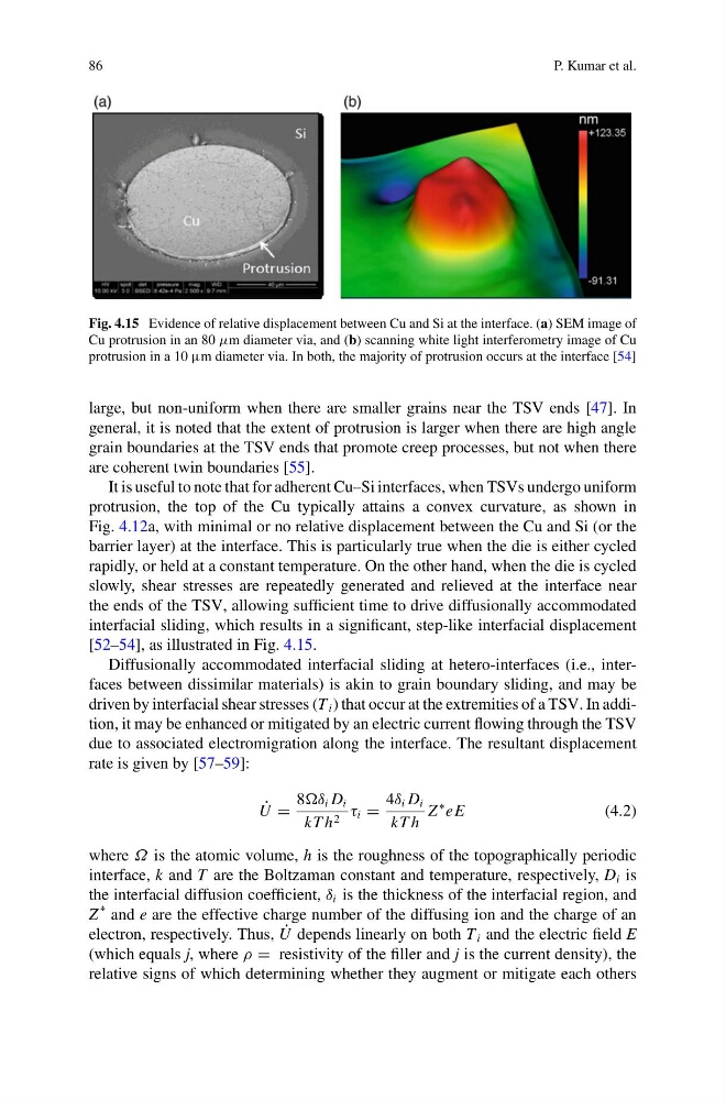
Fig. 4.15 Evidence of relative displacement between Cu and Si at the interface. (a) SEM image of
Cu protrusion in an 80 μm diameter via, and (b) scanning white light interferometry image of Cu
protrusion in a 10 µm diameter via. In both, the majority of protrusion occurs at the interface [54]
large, but non-uniform when there are smaller grains near the TSV ends [47]. In
general, it is noted that the extent of protrusion is larger when there are high angle
grain boundaries at the TSV ends that promote creep processes, but not when there
are coherent twin boundaries [55].
It is useful to note that for adherent Cu–Si interfaces, when TSVs undergo uniform
protrusion, the top of the Cu typically attains a convex curvature, as shown in
Fig. 4.12a, with minimal or no relative displacement between the Cu and Si (or the
barrier layer) at the interface. This is particularly true when the die is either cycled
rapidly, or held at a constant temperature. On the other hand, when the die is cycled
slowly, shear stresses are repeatedly generated and relieved at the interface near
the ends of the TSV, allowing sufficient time to drive diffusionally accommodated
interfacial sliding, which results in a significant, step-like interfacial displacement
[52–54], as illustrated in Fig. 4.15.
Diffusionally accommodated interfacial sliding at hetero-interfaces (i.e., interfaces between dissimilar materials) is akin to grain boundary sliding, and may be
driven by interfacial shear stresses (T i ) that occur at the extremities of a TSV. In addition, it may be enhanced or mitigated by an electric current flowing through the TSV
due to associated electromigration along the interface. The resultant displacement
rate is given by [57–59]:
˙
U =
8δ i D i
kT h 2 τ i =
4δ i D i
kT h
Z
∗ eE
(4.2)
where Ω is the atomic volume, h is the roughness of the topographically periodic
interface, k and T are the Boltzaman constant and temperature, respectively, D i is
the interfacial diffusion coefficient, δ i is the thickness of the interfacial region, and
Z
* and e are the effective charge number of the diffusing ion and the charge of an
electron, respectively. Thus, ˙
U depends linearly on both T i and the electric field E
(which equals j, where ρ = resistivity of the filler and j is the current density), the
relative signs of which determining whether they augment or mitigate each others
P. Kumar et al.
Fig. 4.15 Evidence of relative displacement between Cu and Si at the interface. (a) SEM image of
Cu protrusion in an 80 μm diameter via, and (b) scanning white light interferometry image of Cu
protrusion in a 10 µm diameter via. In both, the majority of protrusion occurs at the interface [54]
large, but non-uniform when there are smaller grains near the TSV ends [47]. In
general, it is noted that the extent of protrusion is larger when there are high angle
grain boundaries at the TSV ends that promote creep processes, but not when there
are coherent twin boundaries [55].
It is useful to note that for adherent Cu–Si interfaces, when TSVs undergo uniform
protrusion, the top of the Cu typically attains a convex curvature, as shown in
Fig. 4.12a, with minimal or no relative displacement between the Cu and Si (or the
barrier layer) at the interface. This is particularly true when the die is either cycled
rapidly, or held at a constant temperature. On the other hand, when the die is cycled
slowly, shear stresses are repeatedly generated and relieved at the interface near
the ends of the TSV, allowing sufficient time to drive diffusionally accommodated
interfacial sliding, which results in a significant, step-like interfacial displacement
[52–54], as illustrated in Fig. 4.15.
Diffusionally accommodated interfacial sliding at hetero-interfaces (i.e., interfaces between dissimilar materials) is akin to grain boundary sliding, and may be
driven by interfacial shear stresses (T i ) that occur at the extremities of a TSV. In addition, it may be enhanced or mitigated by an electric current flowing through the TSV
due to associated electromigration along the interface. The resultant displacement
rate is given by [57–59]:
˙
U =
8δ i D i
kT h 2 τ i =
4δ i D i
kT h
Z
∗ eE
(4.2)
where Ω is the atomic volume, h is the roughness of the topographically periodic
interface, k and T are the Boltzaman constant and temperature, respectively, D i is
the interfacial diffusion coefficient, δ i is the thickness of the interfacial region, and
Z
* and e are the effective charge number of the diffusing ion and the charge of an
electron, respectively. Thus, ˙
U depends linearly on both T i and the electric field E
(which equals j, where ρ = resistivity of the filler and j is the current density), the
relative signs of which determining whether they augment or mitigate each others