

520
V. S. Simi et al.
the electric field strength experienced across the formed oxide and thus affecting
the ions migration and ultimately the diameter of the nanotubes [53]. A linear relationship exists between the diameter and the applied potential [54] and also to the
thickness of the barrier layer at the base of the nanotubes [55]. The potential applied
has a direct effect on the rates of oxidation and dissolution reactions that takes place
during the nanotube formation. Cai et al. [56] reported that the nanotube diameter, at
the tube mouth and bottom are directly proportional to the applied potential. It was
also mentioned that anodically grown nanotubular layers will only be generated, if
the applied potential is kept within the range dictated by the chemical dissolution
activity of the electrolyte. If the potential is too low, the induced rates of oxidation
and dissolution occur too slowly relative to the chemical etching performed by the
electrolyte, leading to the formation of pits and not the oxide layer. If the potential is
too high, field-assisted oxidation occurs too quickly relative to the chemical dissolution of the metallic substrate, which results in the formation of disturbed oxide
layer rather than the nanotubular layer [57]. Sulka et al. [58] extensively studied
the influence of anodizing potential on the structural parameters of porous anodic
titania including pore diameter, inter pore distance, wall thickness, porosity and pore
density.
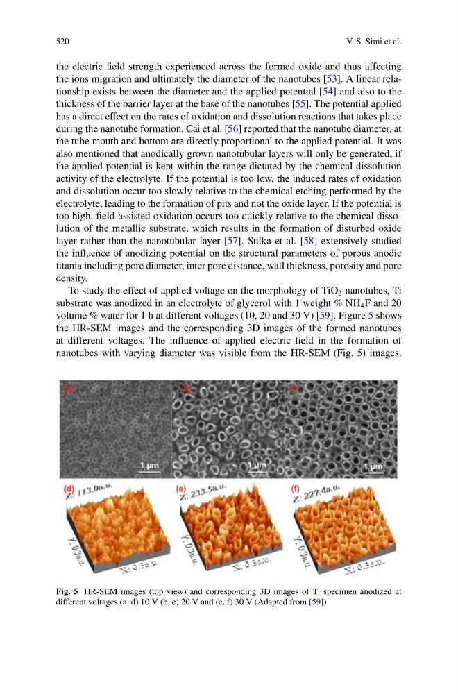
To study the effect of applied voltage on the morphology of TiO 2 nanotubes, Ti
substrate was anodized in an electrolyte of glycerol with 1 weight % NH 4 F and 20
volume % water for 1 h at different voltages (10, 20 and 30 V) [59]. Figure 5 shows
the HR-SEM images and the corresponding 3D images of the formed nanotubes
at different voltages. The influence of applied electric field in the formation of
nanotubes with varying diameter was visible from the HR-SEM (Fig. 5) images.
Fig. 5 HR-SEM images (top view) and corresponding 3D images of Ti specimen anodized at
different voltages (a, d) 10 V (b, e) 20 V and (c, f) 30 V (Adapted from [59])
V. S. Simi et al.
the electric field strength experienced across the formed oxide and thus affecting
the ions migration and ultimately the diameter of the nanotubes [53]. A linear relationship exists between the diameter and the applied potential [54] and also to the
thickness of the barrier layer at the base of the nanotubes [55]. The potential applied
has a direct effect on the rates of oxidation and dissolution reactions that takes place
during the nanotube formation. Cai et al. [56] reported that the nanotube diameter, at
the tube mouth and bottom are directly proportional to the applied potential. It was
also mentioned that anodically grown nanotubular layers will only be generated, if
the applied potential is kept within the range dictated by the chemical dissolution
activity of the electrolyte. If the potential is too low, the induced rates of oxidation
and dissolution occur too slowly relative to the chemical etching performed by the
electrolyte, leading to the formation of pits and not the oxide layer. If the potential is
too high, field-assisted oxidation occurs too quickly relative to the chemical dissolution of the metallic substrate, which results in the formation of disturbed oxide
layer rather than the nanotubular layer [57]. Sulka et al. [58] extensively studied
the influence of anodizing potential on the structural parameters of porous anodic
titania including pore diameter, inter pore distance, wall thickness, porosity and pore
density.
To study the effect of applied voltage on the morphology of TiO 2 nanotubes, Ti
substrate was anodized in an electrolyte of glycerol with 1 weight % NH 4 F and 20
volume % water for 1 h at different voltages (10, 20 and 30 V) [59]. Figure 5 shows
the HR-SEM images and the corresponding 3D images of the formed nanotubes
at different voltages. The influence of applied electric field in the formation of
nanotubes with varying diameter was visible from the HR-SEM (Fig. 5) images.
Fig. 5 HR-SEM images (top view) and corresponding 3D images of Ti specimen anodized at
different voltages (a, d) 10 V (b, e) 20 V and (c, f) 30 V (Adapted from [59])