

Surface Photo-Voltage Spectroscopy: A Versatile Technique …
609
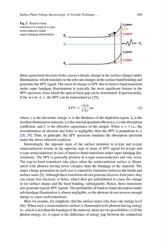
Fig. 2 Band-to-band
transition in a typical n-type
semiconductor under
super-bandgap illumination
photo-generated electrons-holes causes a drastic change in the surface charges under
illumination, which translates to the relevant changes in the surface band bending and
generates the SPV signal. The onset of change in SPV due to band to band transition
under super bandgap illuminations is typically the most significant feature in the
SPV spectrum, from which the optical band gap can be determined. Experimentally,
if the α(λ)w 1, the SPV can be represented as [29],
S PV =
eI 0 w
Chν
ηα
(2)
where, e is the electronic charge, w is the thickness of the depletion region, I 0 is the
incident illumination intensity, η is the internal quantum efficiency, α is the absorption
coefficient, and C is the effective capacitance of the sample. When η = 1 i.e., the
recombination of electron and holes is negligible, then the SPV is proportion to α
[28, 29]. Thus, in principle, the SPV spectrum emulates the absorption spectrum
under the above referred condition.
Interestingly, the opposite signs of the surface potential in p-type and n-type
semiconductors results in the opposite sign of slope of SPV signal for p-type and
n-type semiconductors in case of band-to-band transitions under super bandgap illuminations. The SPV is generally positive in n-type semiconductors and vice versa.
The trap-to-band transitions take place when the semiconductor surface is illuminated with photons having lower energies than the bandgap of the material. The
major charge generation in such case is caused by transitions between the bands and
surface states [9]. Although these transitions do not generate electron–hole pairs, they
can create free electrons or holes, which then get redistributed to cause the change
in net surface charge and the band bending, subsequently. Hence, these transitions
also generate typical SPV signals. The probability of band-to-band absorption under
sub-bandgap illumination is almost negligible, as the photons do not possess enough
energy to cause such transitions.
Here we assume, for simplicity, that the surface states only have one energy level
(Et). When such a semiconductor surface is illuminated with photons having energy
hν, which is less than the bandgap of the material, there are two possibilities: (i) If the
photon energy, hν, is equal to the difference of energy gap between the conduction
609
Fig. 2 Band-to-band
transition in a typical n-type
semiconductor under
super-bandgap illumination
photo-generated electrons-holes causes a drastic change in the surface charges under
illumination, which translates to the relevant changes in the surface band bending and
generates the SPV signal. The onset of change in SPV due to band to band transition
under super bandgap illuminations is typically the most significant feature in the
SPV spectrum, from which the optical band gap can be determined. Experimentally,
if the α(λ)w 1, the SPV can be represented as [29],
S PV =
eI 0 w
Chν
ηα
(2)
where, e is the electronic charge, w is the thickness of the depletion region, I 0 is the
incident illumination intensity, η is the internal quantum efficiency, α is the absorption
coefficient, and C is the effective capacitance of the sample. When η = 1 i.e., the
recombination of electron and holes is negligible, then the SPV is proportion to α
[28, 29]. Thus, in principle, the SPV spectrum emulates the absorption spectrum
under the above referred condition.
Interestingly, the opposite signs of the surface potential in p-type and n-type
semiconductors results in the opposite sign of slope of SPV signal for p-type and
n-type semiconductors in case of band-to-band transitions under super bandgap illuminations. The SPV is generally positive in n-type semiconductors and vice versa.
The trap-to-band transitions take place when the semiconductor surface is illuminated with photons having lower energies than the bandgap of the material. The
major charge generation in such case is caused by transitions between the bands and
surface states [9]. Although these transitions do not generate electron–hole pairs, they
can create free electrons or holes, which then get redistributed to cause the change
in net surface charge and the band bending, subsequently. Hence, these transitions
also generate typical SPV signals. The probability of band-to-band absorption under
sub-bandgap illumination is almost negligible, as the photons do not possess enough
energy to cause such transitions.
Here we assume, for simplicity, that the surface states only have one energy level
(Et). When such a semiconductor surface is illuminated with photons having energy
hν, which is less than the bandgap of the material, there are two possibilities: (i) If the
photon energy, hν, is equal to the difference of energy gap between the conduction