

610
A. Jariwala et al.
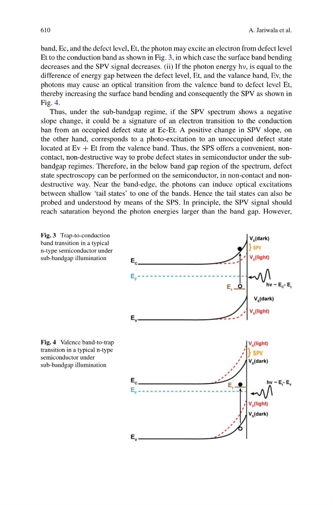
band, Ec, and the defect level, Et, the photon may excite an electron from defect level
Et to the conduction band as shown in Fig. 3, in which case the surface band bending
decreases and the SPV signal decreases. (ii) If the photon energy hν, is equal to the
difference of energy gap between the defect level, Et, and the valance band, Ev, the
photons may cause an optical transition from the valence band to defect level Et,
thereby increasing the surface band bending and consequently the SPV as shown in
Fig. 4.
Thus, under the sub-bandgap regime, if the SPV spectrum shows a negative
slope change, it could be a signature of an electron transition to the conduction
ban from an occupied defect state at Ec-Et. A positive change in SPV slope, on
the other hand, corresponds to a photo-excitation to an unoccupied defect state
located at Ev + Et from the valence band. Thus, the SPS offers a convenient, noncontact, non-destructive way to probe defect states in semiconductor under the subbandgap regimes. Therefore, in the below band gap region of the spectrum, defect
state spectroscopy can be performed on the semiconductor, in non-contact and nondestructive way. Near the band-edge, the photons can induce optical excitations
between shallow ‘tail states’ to one of the bands. Hence the tail states can also be
probed and understood by means of the SPS. In principle, the SPV signal should
reach saturation beyond the photon energies larger than the band gap. However,
Fig. 3 Trap-to-conduction
band transition in a typical
n-type semiconductor under
sub-bandgap illumination
Fig. 4 Valence band-to-trap
transition in a typical n-type
semiconductor under
sub-bandgap illumination
A. Jariwala et al.
band, Ec, and the defect level, Et, the photon may excite an electron from defect level
Et to the conduction band as shown in Fig. 3, in which case the surface band bending
decreases and the SPV signal decreases. (ii) If the photon energy hν, is equal to the
difference of energy gap between the defect level, Et, and the valance band, Ev, the
photons may cause an optical transition from the valence band to defect level Et,
thereby increasing the surface band bending and consequently the SPV as shown in
Fig. 4.
Thus, under the sub-bandgap regime, if the SPV spectrum shows a negative
slope change, it could be a signature of an electron transition to the conduction
ban from an occupied defect state at Ec-Et. A positive change in SPV slope, on
the other hand, corresponds to a photo-excitation to an unoccupied defect state
located at Ev + Et from the valence band. Thus, the SPS offers a convenient, noncontact, non-destructive way to probe defect states in semiconductor under the subbandgap regimes. Therefore, in the below band gap region of the spectrum, defect
state spectroscopy can be performed on the semiconductor, in non-contact and nondestructive way. Near the band-edge, the photons can induce optical excitations
between shallow ‘tail states’ to one of the bands. Hence the tail states can also be
probed and understood by means of the SPS. In principle, the SPV signal should
reach saturation beyond the photon energies larger than the band gap. However,
Fig. 3 Trap-to-conduction
band transition in a typical
n-type semiconductor under
sub-bandgap illumination
Fig. 4 Valence band-to-trap
transition in a typical n-type
semiconductor under
sub-bandgap illumination