

608
A. Jariwala et al.
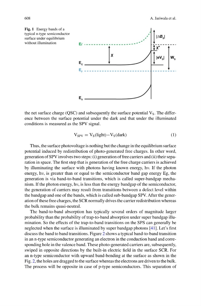
Fig. 1 Energy bands of a
typical n-type semiconductor
surface under equilibrium
without illumination
the net surface charge (QSC) and subsequently the surface potential V S . The difference between the surface potential under the dark and that under the illuminated
conditions is measured as the SPV signal.
V SPV = V S (light)−V S (dark)
(1)
Thus, the surface photovoltage is nothing but the change in the equilibrium surface
potential induced by redistribution of photo-generated free charges. In other word,
generation of SPV involves two steps: (i) generation of free carriers and (ii) their separation in space. The first step that is generation of the free charge carriers is achieved
by illuminating the surface with photons having known energy, hν. If the photon
energy, hν, is greater than or equal to the semiconductor band gap energy Eg, the
generation is via band-to-band transitions, which is called super-bandgap mechanism. If the photon energy, hν, is less than the energy bandgap of the semiconductor,
the generation of carriers may result from transitions between a defect level within
the bandgap and one of the bands, which is called sub-bandgap SPV. After the generation of these free charges, the SCR normally drives the carrier redistribution whereas
the bulk remains quasi-neutral.
The band-to-band absorption has typically several orders of magnitude larger
probability than the probability of trap-to-band absorption under super bandgap illumination. So the effects of the trap-to-band transitions on the SPS can generally be
neglected when the surface is illuminated by super bandgap photons [41]. Let’s first
discuss the band to band transitions. Figure 2 shows a typical band-to-band transition
in an n-type semiconductor generating an electron in the conduction band and corresponding hole in the valence band. These photo-generated carriers are, subsequently,
swiped in opposite directions by the built-in electric field in the surface SCR. For
an n-type semiconductor with upward band-bending at the surface as shown in the
Fig. 2, the holes are dragged to the surface whereas the electrons are driven to the bulk.
The process will be opposite in case of p-type semiconductors. This separation of
A. Jariwala et al.
Fig. 1 Energy bands of a
typical n-type semiconductor
surface under equilibrium
without illumination
the net surface charge (QSC) and subsequently the surface potential V S . The difference between the surface potential under the dark and that under the illuminated
conditions is measured as the SPV signal.
V SPV = V S (light)−V S (dark)
(1)
Thus, the surface photovoltage is nothing but the change in the equilibrium surface
potential induced by redistribution of photo-generated free charges. In other word,
generation of SPV involves two steps: (i) generation of free carriers and (ii) their separation in space. The first step that is generation of the free charge carriers is achieved
by illuminating the surface with photons having known energy, hν. If the photon
energy, hν, is greater than or equal to the semiconductor band gap energy Eg, the
generation is via band-to-band transitions, which is called super-bandgap mechanism. If the photon energy, hν, is less than the energy bandgap of the semiconductor,
the generation of carriers may result from transitions between a defect level within
the bandgap and one of the bands, which is called sub-bandgap SPV. After the generation of these free charges, the SCR normally drives the carrier redistribution whereas
the bulk remains quasi-neutral.
The band-to-band absorption has typically several orders of magnitude larger
probability than the probability of trap-to-band absorption under super bandgap illumination. So the effects of the trap-to-band transitions on the SPS can generally be
neglected when the surface is illuminated by super bandgap photons [41]. Let’s first
discuss the band to band transitions. Figure 2 shows a typical band-to-band transition
in an n-type semiconductor generating an electron in the conduction band and corresponding hole in the valence band. These photo-generated carriers are, subsequently,
swiped in opposite directions by the built-in electric field in the surface SCR. For
an n-type semiconductor with upward band-bending at the surface as shown in the
Fig. 2, the holes are dragged to the surface whereas the electrons are driven to the bulk.
The process will be opposite in case of p-type semiconductors. This separation of