

574
M. Saini et al.
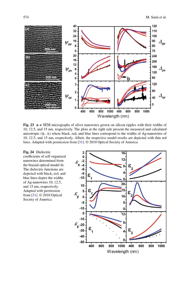
Fig. 23 a–c SEM micrographs of silver nanowires grown on silicon ripples with their widths of
10, 12.5, and 15 nm, respectively. The plots at the right side present the measured and calculated
anisotropic (ψ, ) where black, red, and blue lines correspond to the widths of Ag-nanowires of
10, 12.5, and 15 nm, respectively. Albeit, the respective model results are depicted with thin red
lines. Adapted with permission from [31]. © 2010 Optical Society of America
Fig. 24 Dielectric
coefficients of self-organized
nanowires determined from
the biaxial optical model fit.
The dielectric functions are
depicted with black, red, and
blue lines depict the widths
of Ag-nanowires 10, 12.5,
and 15 nm, respectively.
Adapted with permission
from [31]. © 2010 Optical
Society of America
M. Saini et al.
Fig. 23 a–c SEM micrographs of silver nanowires grown on silicon ripples with their widths of
10, 12.5, and 15 nm, respectively. The plots at the right side present the measured and calculated
anisotropic (ψ, ) where black, red, and blue lines correspond to the widths of Ag-nanowires of
10, 12.5, and 15 nm, respectively. Albeit, the respective model results are depicted with thin red
lines. Adapted with permission from [31]. © 2010 Optical Society of America
Fig. 24 Dielectric
coefficients of self-organized
nanowires determined from
the biaxial optical model fit.
The dielectric functions are
depicted with black, red, and
blue lines depict the widths
of Ag-nanowires 10, 12.5,
and 15 nm, respectively.
Adapted with permission
from [31]. © 2010 Optical
Society of America