

Solid State Physics
281
p-type
e c
e c
e f
n-type
e f
e v
e v
(a)
–
V
+
+
+
+
+
+
– – – – –
Depletion region
(b)
0
– x p
x n
– n e
p
n e
e
(c)
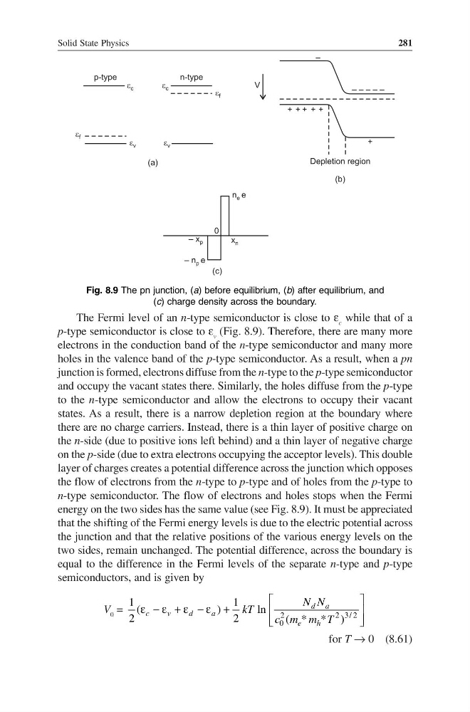
Fig. 8.9 The pn junction, (a) before equilibrium, (b) after equilibrium, and
(c) charge density across the boundary.
The Fermi level of an n-type semiconductor is close to ε c while that of a
p-type semiconductor is close to ε v (Fig. 8.9). Therefore, there are many more
electrons in the conduction band of the n-type semiconductor and many more
holes in the valence band of the p-type semiconductor. As a result, when a pn
junction is formed, electrons diffuse from the n-type to the p-type semiconductor
and occupy the vacant states there. Similarly, the holes diffuse from the p-type
to the n-type semiconductor and allow the electrons to occupy their vacant
states. As a result, there is a narrow depletion region at the boundary where
there are no charge carriers. Instead, there is a thin layer of positive charge on
the n-side (due to positive ions left behind) and a thin layer of negative charge
on the p-side (due to extra electrons occupying the acceptor levels). This double
layer of charges creates a potential difference across the junction which opposes
the flow of electrons from the n-type to p-type and of holes from the p-type to
n-type semiconductor. The flow of electrons and holes stops when the Fermi
energy on the two sides has the same value (see Fig. 8.9). It must be appreciated
that the shifting of the Fermi energy levels is due to the electric potential across
the junction and that the relative positions of the various energy levels on the
two sides, remain unchanged. The potential difference, across the boundary is
equal to the difference in the Fermi levels of the separate n-type and p-type
semiconductors, and is given by
V 0 =
2
23 / 2
0
1
1
(
)
l n
2
2
( * * )
ε − ε + ε − ε +
d a
c
v
d
a
e
h
N N
kT
c m m T
for T → 0 (8.61)
281
p-type
e c
e c
e f
n-type
e f
e v
e v
(a)
–
V
+
+
+
+
+
+
– – – – –
Depletion region
(b)
0
– x p
x n
– n e
p
n e
e
(c)
Fig. 8.9 The pn junction, (a) before equilibrium, (b) after equilibrium, and
(c) charge density across the boundary.
The Fermi level of an n-type semiconductor is close to ε c while that of a
p-type semiconductor is close to ε v (Fig. 8.9). Therefore, there are many more
electrons in the conduction band of the n-type semiconductor and many more
holes in the valence band of the p-type semiconductor. As a result, when a pn
junction is formed, electrons diffuse from the n-type to the p-type semiconductor
and occupy the vacant states there. Similarly, the holes diffuse from the p-type
to the n-type semiconductor and allow the electrons to occupy their vacant
states. As a result, there is a narrow depletion region at the boundary where
there are no charge carriers. Instead, there is a thin layer of positive charge on
the n-side (due to positive ions left behind) and a thin layer of negative charge
on the p-side (due to extra electrons occupying the acceptor levels). This double
layer of charges creates a potential difference across the junction which opposes
the flow of electrons from the n-type to p-type and of holes from the p-type to
n-type semiconductor. The flow of electrons and holes stops when the Fermi
energy on the two sides has the same value (see Fig. 8.9). It must be appreciated
that the shifting of the Fermi energy levels is due to the electric potential across
the junction and that the relative positions of the various energy levels on the
two sides, remain unchanged. The potential difference, across the boundary is
equal to the difference in the Fermi levels of the separate n-type and p-type
semiconductors, and is given by
V 0 =
2
23 / 2
0
1
1
(
)
l n
2
2
( * * )
ε − ε + ε − ε +
d a
c
v
d
a
e
h
N N
kT
c m m T
for T → 0 (8.61)