

Elements of Modern Physics
280
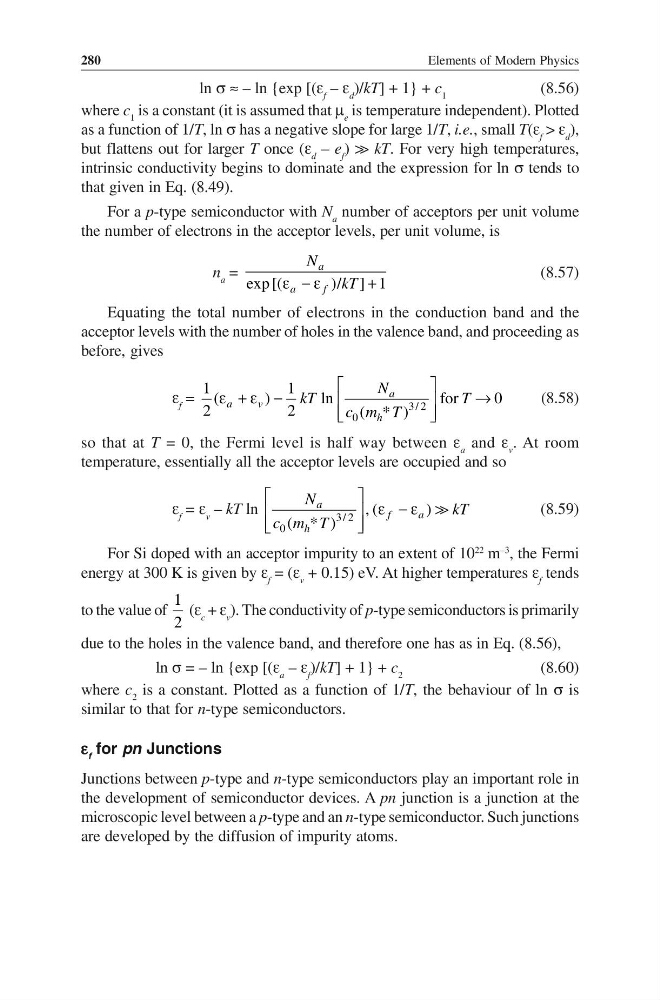
ln σ ≈ – ln {exp [(ε f – ε d )/kT] + 1} + c 1
(8.56)
where c 1 is a constant (it is assumed that µ e is temperature independent). Plotted
as a function of 1/T, ln σ has a negative slope for large 1/T, i.e., small T(ε f > ε d ),
but flattens out for larger T once (ε d – e f ) >> kT. For very high temperatures,
intrinsic conductivity begins to dominate and the expression for ln σ tends to
that given in Eq. (8.49).
For a p-type semiconductor with N a number of acceptors per unit volume
the number of electrons in the acceptor levels, per unit volume, is
n a = exp [(
)/ ] 1
ε − ε
+
a
a
f
N
kT
(8.57)
Equating the total number of electrons in the conduction band and the
acceptor levels with the number of holes in the valence band, and proceeding as
before, gives
ε f =
3 / 2
0
1
1
(
)
ln
for
0
2
2
( * )
ε + ε −
→
a
a
v
h
N
kT
T
c m T
(8.58)
so that at T = 0, the Fermi level is half way between ε a and ε v . At room
temperature, essentially all the acceptor levels are occupied and so
ε f = ε v – kT ln
3 / 2
0
, (
)
( * )
ε − ε > >
a
f
a
h
N
kT
c m T
(8.59)
For Si doped with an acceptor impurity to an extent of 10
22
m
–3
, the Fermi
energy at 300 K is given by ε f = (ε v + 0.15) eV. At higher temperatures ε f tends
to the value of
1
2
(ε c + ε v ). The conductivity of p-type semiconductors is primarily
due to the holes in the valence band, and therefore one has as in Eq. (8.56),
ln σ = – ln {exp [(ε a – ε f )/kT] + 1} + c 2
(8.60)
where c 2 is a constant. Plotted as a function of 1/T, the behaviour of ln σ is
similar to that for n-type semiconductors.
ε
ε ε
ε ε f for pn Junctions
Junctions between p-type and n-type semiconductors play an important role in
the development of semiconductor devices. A pn junction is a junction at the
microscopic level between a p-type and an n-type semiconductor. Such junctions
are developed by the diffusion of impurity atoms.
280
ln σ ≈ – ln {exp [(ε f – ε d )/kT] + 1} + c 1
(8.56)
where c 1 is a constant (it is assumed that µ e is temperature independent). Plotted
as a function of 1/T, ln σ has a negative slope for large 1/T, i.e., small T(ε f > ε d ),
but flattens out for larger T once (ε d – e f ) >> kT. For very high temperatures,
intrinsic conductivity begins to dominate and the expression for ln σ tends to
that given in Eq. (8.49).
For a p-type semiconductor with N a number of acceptors per unit volume
the number of electrons in the acceptor levels, per unit volume, is
n a = exp [(
)/ ] 1
ε − ε
+
a
a
f
N
kT
(8.57)
Equating the total number of electrons in the conduction band and the
acceptor levels with the number of holes in the valence band, and proceeding as
before, gives
ε f =
3 / 2
0
1
1
(
)
ln
for
0
2
2
( * )
ε + ε −
→
a
a
v
h
N
kT
T
c m T
(8.58)
so that at T = 0, the Fermi level is half way between ε a and ε v . At room
temperature, essentially all the acceptor levels are occupied and so
ε f = ε v – kT ln
3 / 2
0
, (
)
( * )
ε − ε > >
a
f
a
h
N
kT
c m T
(8.59)
For Si doped with an acceptor impurity to an extent of 10
22
m
–3
, the Fermi
energy at 300 K is given by ε f = (ε v + 0.15) eV. At higher temperatures ε f tends
to the value of
1
2
(ε c + ε v ). The conductivity of p-type semiconductors is primarily
due to the holes in the valence band, and therefore one has as in Eq. (8.56),
ln σ = – ln {exp [(ε a – ε f )/kT] + 1} + c 2
(8.60)
where c 2 is a constant. Plotted as a function of 1/T, the behaviour of ln σ is
similar to that for n-type semiconductors.
ε
ε ε
ε ε f for pn Junctions
Junctions between p-type and n-type semiconductors play an important role in
the development of semiconductor devices. A pn junction is a junction at the
microscopic level between a p-type and an n-type semiconductor. Such junctions
are developed by the diffusion of impurity atoms.