

Elements of Modern Physics
282
and
V 0 = ε c – ε v + kT ln 2
23 / 2
0 ( * * )
d a
e
h
N N
c m m T
(8.62)
at room temperature.
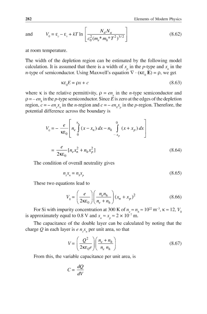
The width of the depletion region can be estimated by the following model
calculation. It is assumed that there is a width of x p in the p-type and x n in the
n-type of semiconductor. Using Maxwell’s equation ∇ ⋅ (κε 0 E) = ρ, we get
κε 0 E = ρx + c
(8.63)
where κ is the relative permittivity, ρ = en e in the n-type semiconductor and
ρ = – en h in the p-type semiconductor. Since E is zero at the edges of the depletion
region, c = – en e x n in the n-region and c = – en h x p in the p-region. Therefore, the
potential difference across the boundary is
V 0 = –
0
0
0
(
)
(
)
−
−
−
+
κε
∫
∫
n
p
x
e
n
h
p
x
e n
x x dx n
x x dx
=
2
2
0
[
]
2
+
κε
e n
h p
e n x
n x
(8.64)
The condition of overall neutrality gives
n e x n = n h x p
(8.65)
These two equations lead to
V 0 =
2
0
(
)
2
+
κε
+
e h
n
p
e
h
n n
e
x x
n n
(8.66)
For Si with impurity concentration at 300 K of n e ≈ n h ≈ 10
22
m
–3
, κ ≈ 12, V 0
is approximately equal to 0.8 V and x n ≈ x p ≈ 2 × 10
–7
m.
The capacitance of the double layer can be calculated by noting that the
charge Q in each layer is e n e x n per unit area, so that
V =
2
0
2
+
κε
e
h
e h
n n
Q
e
n n
(8.67)
From this, the variable capacitance per unit area, is
C =
dQ
dV
282
and
V 0 = ε c – ε v + kT ln 2
23 / 2
0 ( * * )
d a
e
h
N N
c m m T
(8.62)
at room temperature.
The width of the depletion region can be estimated by the following model
calculation. It is assumed that there is a width of x p in the p-type and x n in the
n-type of semiconductor. Using Maxwell’s equation ∇ ⋅ (κε 0 E) = ρ, we get
κε 0 E = ρx + c
(8.63)
where κ is the relative permittivity, ρ = en e in the n-type semiconductor and
ρ = – en h in the p-type semiconductor. Since E is zero at the edges of the depletion
region, c = – en e x n in the n-region and c = – en h x p in the p-region. Therefore, the
potential difference across the boundary is
V 0 = –
0
0
0
(
)
(
)
−
−
−
+
κε
∫
∫
n
p
x
e
n
h
p
x
e n
x x dx n
x x dx
=
2
2
0
[
]
2
+
κε
e n
h p
e n x
n x
(8.64)
The condition of overall neutrality gives
n e x n = n h x p
(8.65)
These two equations lead to
V 0 =
2
0
(
)
2
+
κε
+
e h
n
p
e
h
n n
e
x x
n n
(8.66)
For Si with impurity concentration at 300 K of n e ≈ n h ≈ 10
22
m
–3
, κ ≈ 12, V 0
is approximately equal to 0.8 V and x n ≈ x p ≈ 2 × 10
–7
m.
The capacitance of the double layer can be calculated by noting that the
charge Q in each layer is e n e x n per unit area, so that
V =
2
0
2
+
κε
e
h
e h
n n
Q
e
n n
(8.67)
From this, the variable capacitance per unit area, is
C =
dQ
dV