

66
W. C. Law and S. De W. Wong
lower when switching from the parallel to anti-parallel configuration [112, 113, 114].
This can be explained by the free layer attempting to polarize the conduction electrons
as they travel towards the reference layer, reducing the amount of the minority carriers
that will backscatter at the reference layer.
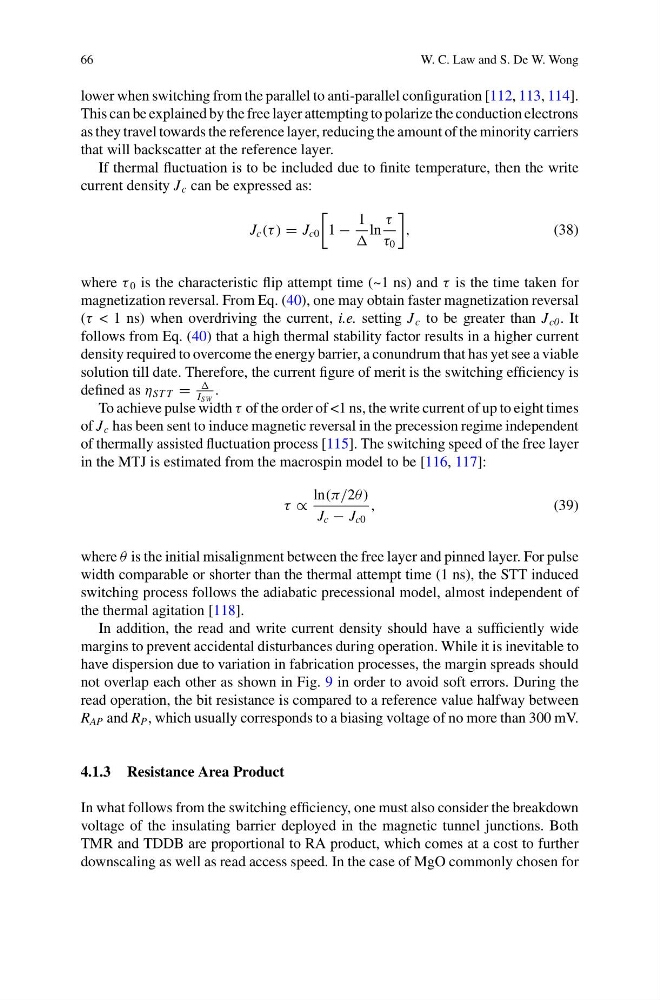
If thermal fluctuation is to be included due to finite temperature, then the write
current density J c can be expressed as:
J c (τ ) = J c0
1 −
1
ln
τ
τ 0
,
(38)
where τ 0 is the characteristic flip attempt time (~1 ns) and τ is the time taken for
magnetization reversal. From Eq. (40), one may obtain faster magnetization reversal
(τ < 1 ns) when overdriving the current, i.e. setting J c to be greater than J c0 . It
follows from Eq. (40) that a high thermal stability factor results in a higher current
density required to overcome the energy barrier, a conundrum that has yet see a viable
solution till date. Therefore, the current figure of merit is the switching efficiency is
defined as η ST T =
I SW
.
To achieve pulse width τ of the order of <1 ns, the write current of up to eight times
of J c has been sent to induce magnetic reversal in the precession regime independent
of thermally assisted fluctuation process [115]. The switching speed of the free layer
in the MTJ is estimated from the macrospin model to be [116, 117]:
τ ∝
ln(π/2θ)
J c − J c0
,
(39)
where θ is the initial misalignment between the free layer and pinned layer. For pulse
width comparable or shorter than the thermal attempt time (1 ns), the STT induced
switching process follows the adiabatic precessional model, almost independent of
the thermal agitation [118].
In addition, the read and write current density should have a sufficiently wide
margins to prevent accidental disturbances during operation. While it is inevitable to
have dispersion due to variation in fabrication processes, the margin spreads should
not overlap each other as shown in Fig. 9 in order to avoid soft errors. During the
read operation, the bit resistance is compared to a reference value halfway between
R AP and R P , which usually corresponds to a biasing voltage of no more than 300 mV.
4.1.3 Resistance Area Product
In what follows from the switching efficiency, one must also consider the breakdown
voltage of the insulating barrier deployed in the magnetic tunnel junctions. Both
TMR and TDDB are proportional to RA product, which comes at a cost to further
downscaling as well as read access speed. In the case of MgO commonly chosen for
W. C. Law and S. De W. Wong
lower when switching from the parallel to anti-parallel configuration [112, 113, 114].
This can be explained by the free layer attempting to polarize the conduction electrons
as they travel towards the reference layer, reducing the amount of the minority carriers
that will backscatter at the reference layer.
If thermal fluctuation is to be included due to finite temperature, then the write
current density J c can be expressed as:
J c (τ ) = J c0
1 −
1
ln
τ
τ 0
,
(38)
where τ 0 is the characteristic flip attempt time (~1 ns) and τ is the time taken for
magnetization reversal. From Eq. (40), one may obtain faster magnetization reversal
(τ < 1 ns) when overdriving the current, i.e. setting J c to be greater than J c0 . It
follows from Eq. (40) that a high thermal stability factor results in a higher current
density required to overcome the energy barrier, a conundrum that has yet see a viable
solution till date. Therefore, the current figure of merit is the switching efficiency is
defined as η ST T =
I SW
.
To achieve pulse width τ of the order of <1 ns, the write current of up to eight times
of J c has been sent to induce magnetic reversal in the precession regime independent
of thermally assisted fluctuation process [115]. The switching speed of the free layer
in the MTJ is estimated from the macrospin model to be [116, 117]:
τ ∝
ln(π/2θ)
J c − J c0
,
(39)
where θ is the initial misalignment between the free layer and pinned layer. For pulse
width comparable or shorter than the thermal attempt time (1 ns), the STT induced
switching process follows the adiabatic precessional model, almost independent of
the thermal agitation [118].
In addition, the read and write current density should have a sufficiently wide
margins to prevent accidental disturbances during operation. While it is inevitable to
have dispersion due to variation in fabrication processes, the margin spreads should
not overlap each other as shown in Fig. 9 in order to avoid soft errors. During the
read operation, the bit resistance is compared to a reference value halfway between
R AP and R P , which usually corresponds to a biasing voltage of no more than 300 mV.
4.1.3 Resistance Area Product
In what follows from the switching efficiency, one must also consider the breakdown
voltage of the insulating barrier deployed in the magnetic tunnel junctions. Both
TMR and TDDB are proportional to RA product, which comes at a cost to further
downscaling as well as read access speed. In the case of MgO commonly chosen for