

Spin Transfer Torque Magnetoresistive Random Access Memory
67
a
b
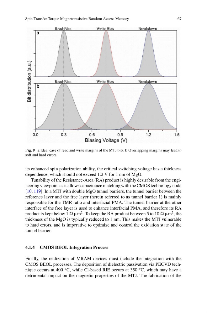
Fig. 9 a Ideal case of read and write margins of the MTJ bits. b Overlapping margins may lead to
soft and hard errors
its enhanced spin polarization ability, the critical switching voltage has a thickness
dependence, which should not exceed 1.2 V for 1 nm of MgO.
Tunability of the Resistance-Area (RA) product is highly desirable from the engineering viewpoint as it allows capacitance matching with the CMOS technology node
[10, 119]. In a MTJ with double MgO tunnel barriers, the tunnel barrier between the
reference layer and the free layer (herein referred to as tunnel barrier 1) is mainly
responsible for the TMR ratio and interfacial PMA. The tunnel barrier at the other
interface of the free layer is used to enhance interfacial PMA, and therefore its RA
product is kept below 1 μm
2 . To keep the RA product between 5 to 10 μm
2 , the
thickness of the MgO is typically reduced to 1 nm. This makes the MTJ vulnerable
to hard errors, and is imperative to optimize and control the oxidation state of the
tunnel barrier.
4.1.4 CMOS BEOL Integration Process
Finally, the realization of MRAM devices must include the integration with the
CMOS BEOL processes. The deposition of dielectric passivation via PECVD technique occurs at 400 °C, while Cl-based RIE occurs at 350 °C, which may have a
detrimental impact on the magnetic properties of the MTJ. The fabrication of the
67
a
b
Fig. 9 a Ideal case of read and write margins of the MTJ bits. b Overlapping margins may lead to
soft and hard errors
its enhanced spin polarization ability, the critical switching voltage has a thickness
dependence, which should not exceed 1.2 V for 1 nm of MgO.
Tunability of the Resistance-Area (RA) product is highly desirable from the engineering viewpoint as it allows capacitance matching with the CMOS technology node
[10, 119]. In a MTJ with double MgO tunnel barriers, the tunnel barrier between the
reference layer and the free layer (herein referred to as tunnel barrier 1) is mainly
responsible for the TMR ratio and interfacial PMA. The tunnel barrier at the other
interface of the free layer is used to enhance interfacial PMA, and therefore its RA
product is kept below 1 μm
2 . To keep the RA product between 5 to 10 μm
2 , the
thickness of the MgO is typically reduced to 1 nm. This makes the MTJ vulnerable
to hard errors, and is imperative to optimize and control the oxidation state of the
tunnel barrier.
4.1.4 CMOS BEOL Integration Process
Finally, the realization of MRAM devices must include the integration with the
CMOS BEOL processes. The deposition of dielectric passivation via PECVD technique occurs at 400 °C, while Cl-based RIE occurs at 350 °C, which may have a
detrimental impact on the magnetic properties of the MTJ. The fabrication of the