

RRAM Device Characterizations and Modelling
367
0.0
0.3
0.6
0.9
1.2
0.00
0.05
0.10
0.15
Normalized Current(a.u.)
Voltage(V)
w decrease
(b)
0.0
0.3
0.6
0.9
1.2
10
-4
10
-3
10
-2
10
-1
10
0
Normalized Current(a.u.)
Voltage(V)
x increase
(c)
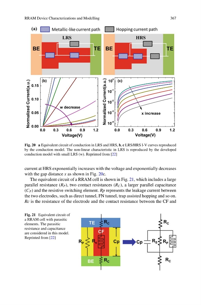
Fig. 20 a Equivalent circuit of conduction in LRS and HRS, b, c LRS/HRS I-V curves reproduced
by the conduction model. The non-linear characteristic in LRS is reproduced by the developed
conduction model with small LRS (w). Reprinted from [22]
current at HRS exponentially increases with the voltage and exponentially decreases
with the gap distance x as shown in Fig. 20c.
The equivalent circuit of a RRAM cell is shown in Fig. 21, which includes a large
parallel resistance (R P ), two contact resistances (R C ), a larger parallel capacitance
(C P ) and the resistive switching element. Rp represents the leakage current between
the two electrodes, such as direct tunnel, FN tunnel, trap assisted hopping and so on.
Rc is the resistance of the electrode and the contact resistance between the CF and
Fig. 21 Equivalent circuit of
a RRAM cell with parasitic
elements. The parasitic
resistance and capacitance
are considered in this model.
Reprinted from [22]
367
0.0
0.3
0.6
0.9
1.2
0.00
0.05
0.10
0.15
Normalized Current(a.u.)
Voltage(V)
w decrease
(b)
0.0
0.3
0.6
0.9
1.2
10
-4
10
-3
10
-2
10
-1
10
0
Normalized Current(a.u.)
Voltage(V)
x increase
(c)
Fig. 20 a Equivalent circuit of conduction in LRS and HRS, b, c LRS/HRS I-V curves reproduced
by the conduction model. The non-linear characteristic in LRS is reproduced by the developed
conduction model with small LRS (w). Reprinted from [22]
current at HRS exponentially increases with the voltage and exponentially decreases
with the gap distance x as shown in Fig. 20c.
The equivalent circuit of a RRAM cell is shown in Fig. 21, which includes a large
parallel resistance (R P ), two contact resistances (R C ), a larger parallel capacitance
(C P ) and the resistive switching element. Rp represents the leakage current between
the two electrodes, such as direct tunnel, FN tunnel, trap assisted hopping and so on.
Rc is the resistance of the electrode and the contact resistance between the CF and
Fig. 21 Equivalent circuit of
a RRAM cell with parasitic
elements. The parasitic
resistance and capacitance
are considered in this model.
Reprinted from [22]