

Resistive Random Access Memory Device …
331
with increasing array size due to more current leakage paths, causing memory performance degradation. To suppress this sneak path problem, a prevalent solution at the
device level is to incorporate a selection device with each RRAM device such as a
transistor or a nonlinear selector, to get a 1T1R or 1S1R configuration, respectively.
Another key requirement for crosspoint memory arrays is high scalability such
that the storage capacity can meet the specifications driven by the growth of internet
data, data centers and mobile computers. A seemingly straightforward solution is
to decrease the individual cell size such as reducing the RRAM device diameter.
However, this raises concerns regarding increased spatial and temporal variability
in the RRAM devices contained in the crosspoint array. Also, the interconnect and
peripheral circuit area should decrease with downscaling which will increase series
resistance due to geometry scaling and increased surface scattering [113], resulting in
operational problems at high operating currents. Several methods have been reported
to reduce interconnect resistance such as using graphene and carbon nanotubes as
interconnect materials [114].
In order to circumvent the problems in downscaling, unique three-dimensional
(3D) array architectures have been proposed such as the horizontal stacked 3D and
vertical 3D structures. By stacking multiple 2D layers of memory crosspoint (Fig. 7)
into a 3D structure, the minimal feature size is further reduced to 4F
2 /n, where n is the
number of stacked layers. Between these two 3D structures, the vertical configuration
has higher processing yield and cost effectiveness since only one critical lithography
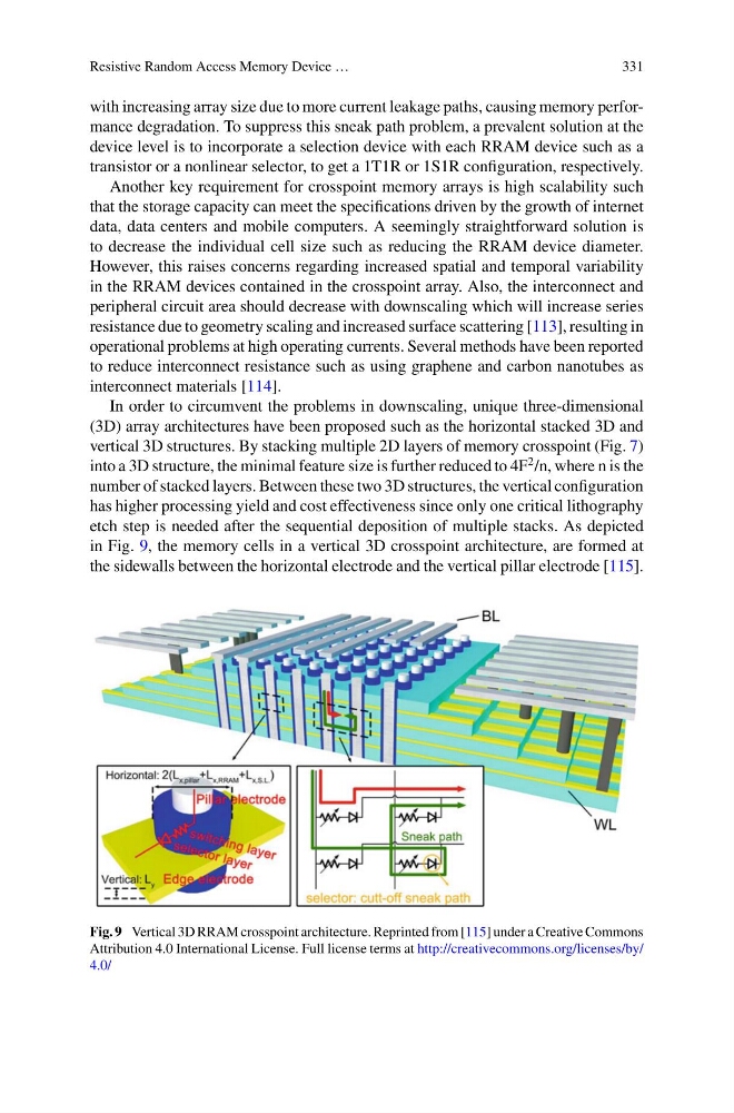
etch step is needed after the sequential deposition of multiple stacks. As depicted
in Fig. 9, the memory cells in a vertical 3D crosspoint architecture, are formed at
the sidewalls between the horizontal electrode and the vertical pillar electrode [115].
Fig. 9 Vertical 3D RRAM crosspoint architecture. Reprinted from [115] under a Creative Commons
Attribution 4.0 International License. Full license terms at http://creativecommons.org/licenses/by/
4.0/
331
with increasing array size due to more current leakage paths, causing memory performance degradation. To suppress this sneak path problem, a prevalent solution at the
device level is to incorporate a selection device with each RRAM device such as a
transistor or a nonlinear selector, to get a 1T1R or 1S1R configuration, respectively.
Another key requirement for crosspoint memory arrays is high scalability such
that the storage capacity can meet the specifications driven by the growth of internet
data, data centers and mobile computers. A seemingly straightforward solution is
to decrease the individual cell size such as reducing the RRAM device diameter.
However, this raises concerns regarding increased spatial and temporal variability
in the RRAM devices contained in the crosspoint array. Also, the interconnect and
peripheral circuit area should decrease with downscaling which will increase series
resistance due to geometry scaling and increased surface scattering [113], resulting in
operational problems at high operating currents. Several methods have been reported
to reduce interconnect resistance such as using graphene and carbon nanotubes as
interconnect materials [114].
In order to circumvent the problems in downscaling, unique three-dimensional
(3D) array architectures have been proposed such as the horizontal stacked 3D and
vertical 3D structures. By stacking multiple 2D layers of memory crosspoint (Fig. 7)
into a 3D structure, the minimal feature size is further reduced to 4F
2 /n, where n is the
number of stacked layers. Between these two 3D structures, the vertical configuration
has higher processing yield and cost effectiveness since only one critical lithography
etch step is needed after the sequential deposition of multiple stacks. As depicted
in Fig. 9, the memory cells in a vertical 3D crosspoint architecture, are formed at
the sidewalls between the horizontal electrode and the vertical pillar electrode [115].
Fig. 9 Vertical 3D RRAM crosspoint architecture. Reprinted from [115] under a Creative Commons
Attribution 4.0 International License. Full license terms at http://creativecommons.org/licenses/by/
4.0/