

330
V. Y. Zhuo et al.
3 RRAM Crosspoint Array
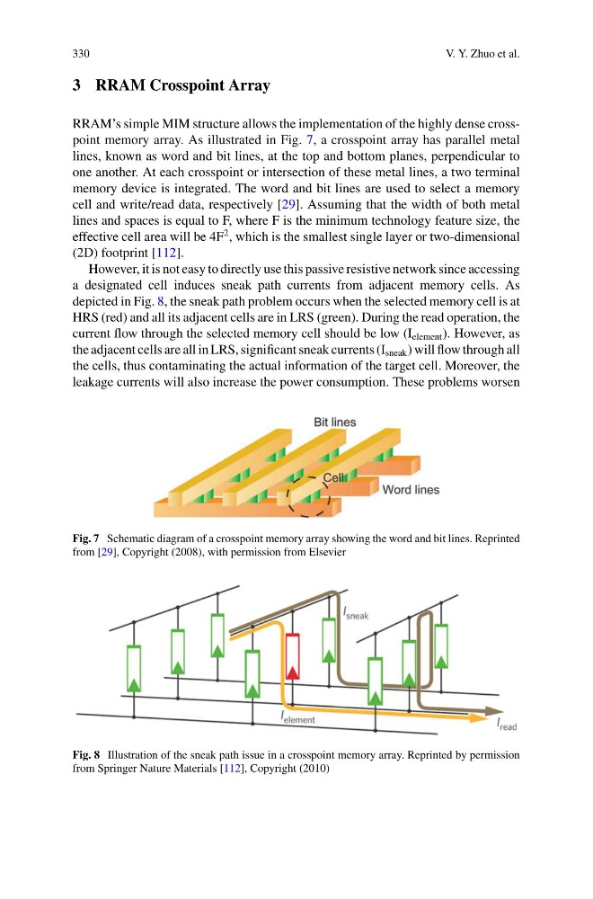
RRAM’s simple MIM structure allows the implementation of the highly dense crosspoint memory array. As illustrated in Fig. 7, a crosspoint array has parallel metal
lines, known as word and bit lines, at the top and bottom planes, perpendicular to
one another. At each crosspoint or intersection of these metal lines, a two terminal
memory device is integrated. The word and bit lines are used to select a memory
cell and write/read data, respectively [29]. Assuming that the width of both metal
lines and spaces is equal to F, where F is the minimum technology feature size, the
effective cell area will be 4F
2 , which is the smallest single layer or two-dimensional
(2D) footprint [112].
However, it is not easy to directly use this passive resistive network since accessing
a designated cell induces sneak path currents from adjacent memory cells. As
depicted in Fig. 8, the sneak path problem occurs when the selected memory cell is at
HRS (red) and all its adjacent cells are in LRS (green). During the read operation, the
current flow through the selected memory cell should be low (I element ). However, as
the adjacent cells are all in LRS, significant sneak currents (I sneak ) will flow through all
the cells, thus contaminating the actual information of the target cell. Moreover, the
leakage currents will also increase the power consumption. These problems worsen
Fig. 7 Schematic diagram of a crosspoint memory array showing the word and bit lines. Reprinted
from [29], Copyright (2008), with permission from Elsevier
Fig. 8 Illustration of the sneak path issue in a crosspoint memory array. Reprinted by permission
from Springer Nature Materials [112], Copyright (2010)
V. Y. Zhuo et al.
3 RRAM Crosspoint Array
RRAM’s simple MIM structure allows the implementation of the highly dense crosspoint memory array. As illustrated in Fig. 7, a crosspoint array has parallel metal
lines, known as word and bit lines, at the top and bottom planes, perpendicular to
one another. At each crosspoint or intersection of these metal lines, a two terminal
memory device is integrated. The word and bit lines are used to select a memory
cell and write/read data, respectively [29]. Assuming that the width of both metal
lines and spaces is equal to F, where F is the minimum technology feature size, the
effective cell area will be 4F
2 , which is the smallest single layer or two-dimensional
(2D) footprint [112].
However, it is not easy to directly use this passive resistive network since accessing
a designated cell induces sneak path currents from adjacent memory cells. As
depicted in Fig. 8, the sneak path problem occurs when the selected memory cell is at
HRS (red) and all its adjacent cells are in LRS (green). During the read operation, the
current flow through the selected memory cell should be low (I element ). However, as
the adjacent cells are all in LRS, significant sneak currents (I sneak ) will flow through all
the cells, thus contaminating the actual information of the target cell. Moreover, the
leakage currents will also increase the power consumption. These problems worsen
Fig. 7 Schematic diagram of a crosspoint memory array showing the word and bit lines. Reprinted
from [29], Copyright (2008), with permission from Elsevier
Fig. 8 Illustration of the sneak path issue in a crosspoint memory array. Reprinted by permission
from Springer Nature Materials [112], Copyright (2010)