

Resistive Random Access Memory Device …
329
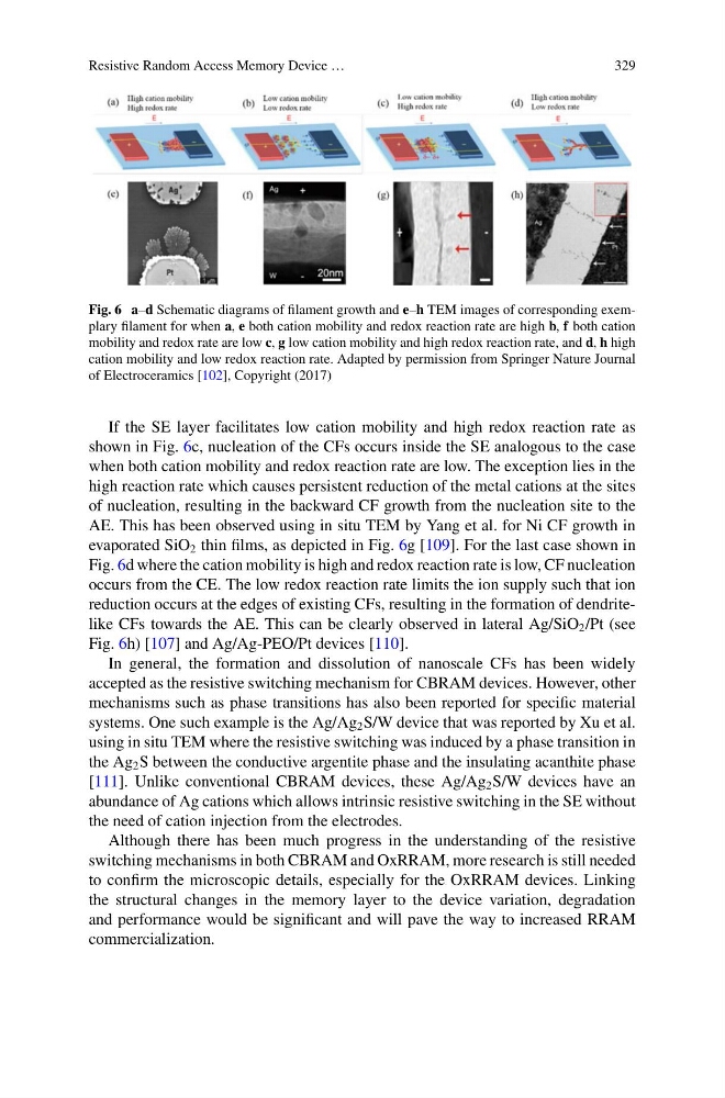
Fig. 6 a–d Schematic diagrams of filament growth and e–h TEM images of corresponding exemplary filament for when a, e both cation mobility and redox reaction rate are high b, f both cation
mobility and redox rate are low c, g low cation mobility and high redox reaction rate, and d, h high
cation mobility and low redox reaction rate. Adapted by permission from Springer Nature Journal
of Electroceramics [102], Copyright (2017)
If the SE layer facilitates low cation mobility and high redox reaction rate as
shown in Fig. 6c, nucleation of the CFs occurs inside the SE analogous to the case
when both cation mobility and redox reaction rate are low. The exception lies in the
high reaction rate which causes persistent reduction of the metal cations at the sites
of nucleation, resulting in the backward CF growth from the nucleation site to the
AE. This has been observed using in situ TEM by Yang et al. for Ni CF growth in
evaporated SiO 2 thin films, as depicted in Fig. 6g [109]. For the last case shown in
Fig. 6d where the cation mobility is high and redox reaction rate is low, CF nucleation
occurs from the CE. The low redox reaction rate limits the ion supply such that ion
reduction occurs at the edges of existing CFs, resulting in the formation of dendritelike CFs towards the AE. This can be clearly observed in lateral Ag/SiO 2 /Pt (see
Fig. 6h) [107] and Ag/Ag-PEO/Pt devices [110].
In general, the formation and dissolution of nanoscale CFs has been widely
accepted as the resistive switching mechanism for CBRAM devices. However, other
mechanisms such as phase transitions has also been reported for specific material
systems. One such example is the Ag/Ag 2 S/W device that was reported by Xu et al.
using in situ TEM where the resistive switching was induced by a phase transition in
the Ag 2 S between the conductive argentite phase and the insulating acanthite phase
[111]. Unlike conventional CBRAM devices, these Ag/Ag 2 S/W devices have an
abundance of Ag cations which allows intrinsic resistive switching in the SE without
the need of cation injection from the electrodes.
Although there has been much progress in the understanding of the resistive
switching mechanisms in both CBRAM and OxRRAM, more research is still needed
to confirm the microscopic details, especially for the OxRRAM devices. Linking
the structural changes in the memory layer to the device variation, degradation
and performance would be significant and will pave the way to increased RRAM
commercialization.
329
Fig. 6 a–d Schematic diagrams of filament growth and e–h TEM images of corresponding exemplary filament for when a, e both cation mobility and redox reaction rate are high b, f both cation
mobility and redox rate are low c, g low cation mobility and high redox reaction rate, and d, h high
cation mobility and low redox reaction rate. Adapted by permission from Springer Nature Journal
of Electroceramics [102], Copyright (2017)
If the SE layer facilitates low cation mobility and high redox reaction rate as
shown in Fig. 6c, nucleation of the CFs occurs inside the SE analogous to the case
when both cation mobility and redox reaction rate are low. The exception lies in the
high reaction rate which causes persistent reduction of the metal cations at the sites
of nucleation, resulting in the backward CF growth from the nucleation site to the
AE. This has been observed using in situ TEM by Yang et al. for Ni CF growth in
evaporated SiO 2 thin films, as depicted in Fig. 6g [109]. For the last case shown in
Fig. 6d where the cation mobility is high and redox reaction rate is low, CF nucleation
occurs from the CE. The low redox reaction rate limits the ion supply such that ion
reduction occurs at the edges of existing CFs, resulting in the formation of dendritelike CFs towards the AE. This can be clearly observed in lateral Ag/SiO 2 /Pt (see
Fig. 6h) [107] and Ag/Ag-PEO/Pt devices [110].
In general, the formation and dissolution of nanoscale CFs has been widely
accepted as the resistive switching mechanism for CBRAM devices. However, other
mechanisms such as phase transitions has also been reported for specific material
systems. One such example is the Ag/Ag 2 S/W device that was reported by Xu et al.
using in situ TEM where the resistive switching was induced by a phase transition in
the Ag 2 S between the conductive argentite phase and the insulating acanthite phase
[111]. Unlike conventional CBRAM devices, these Ag/Ag 2 S/W devices have an
abundance of Ag cations which allows intrinsic resistive switching in the SE without
the need of cation injection from the electrodes.
Although there has been much progress in the understanding of the resistive
switching mechanisms in both CBRAM and OxRRAM, more research is still needed
to confirm the microscopic details, especially for the OxRRAM devices. Linking
the structural changes in the memory layer to the device variation, degradation
and performance would be significant and will pave the way to increased RRAM
commercialization.