

3D Nanomagnetic Logic
289
that a split-stack MR structure can be fabricated in an easy way for direct integration
into pNML. For that, the pNML output magnet serves as the free-layer of the sensor
and we found the concept prospective for future pNML research.
5.4 A Field-Clock as Power Supply
In order to operate the 3D pNML devices, a bipolar magnetic field-clock with constant amplitude over the pNML device-space has to be provided. Clocking amplitudes
are equal to the switching field of the ANC, and range from ≈ 10 mT to 100 mT for
typical Co/Pt films. There might be applications, where an external magnetic field is
conceivable but for pNML computing, the field clock has to be generated on-chip. As
already depicted in Fig. 18, magnetic fields are most efficiently generated by inductors with a ferromagnetic core incorporating a thin slit. By contrast, simple air-coils
can hardly provide the needed clocking amplitude even though lower switching fields
are feasible by using low PMA magnetic stacks [68]. Our concept of pNML clocking
is based on a planar design of a current carrying copper wire, sandwiched between
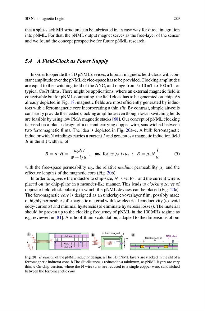
two ferromagnetic films. The idea is depicted in Fig. 20a–c. A bulk ferromagnetic
inductor with N windings carries a current I and generates a magnetic induction field
B in the slit width w of
B = μ 0 H =
μ 0 N I
w + l/μ r
, and for w l/μ r : B = μ 0 N
I
w
(5)
with the free-space permeability μ 0 , the relative medium permeability μ r and the
effective length l of the magnetic core (Fig. 20b).
In order to squeeze the inductor to chip-size, N is set to 1 and the current wire is
placed on the chip-plane in a meander-like manner. This leads to clocking zones of
opposite field-clock polarity in which the pNML devices can be placed (Fig. 20c).
The ferromagnetic core is designed as an underlayer/overlayer film, possibly made
of highly permeable soft-magnetic material with low electrical conductivity (to avoid
eddy-currents) and minimal hysteresis (to eliminate hysteresis losses). The material
should be proven up to the clocking frequency of pNML in the 100 MHz regime as
e.g. reviewed in [81]. A rule-of-thumb calculation, adapted to the dimensions of our
Fig. 20 Evolution of the pNML inductor design. a The 3D pNML layers are stacked in the slit of a
ferromagnetic inductor core. b The slit-distance is reduced to a minimum, as pNML layers are very
thin. c On-chip version, where the N wire turns are reduced to a single copper wire, sandwiched
between the ferromagnetic core
289
that a split-stack MR structure can be fabricated in an easy way for direct integration
into pNML. For that, the pNML output magnet serves as the free-layer of the sensor
and we found the concept prospective for future pNML research.
5.4 A Field-Clock as Power Supply
In order to operate the 3D pNML devices, a bipolar magnetic field-clock with constant amplitude over the pNML device-space has to be provided. Clocking amplitudes
are equal to the switching field of the ANC, and range from ≈ 10 mT to 100 mT for
typical Co/Pt films. There might be applications, where an external magnetic field is
conceivable but for pNML computing, the field clock has to be generated on-chip. As
already depicted in Fig. 18, magnetic fields are most efficiently generated by inductors with a ferromagnetic core incorporating a thin slit. By contrast, simple air-coils
can hardly provide the needed clocking amplitude even though lower switching fields
are feasible by using low PMA magnetic stacks [68]. Our concept of pNML clocking
is based on a planar design of a current carrying copper wire, sandwiched between
two ferromagnetic films. The idea is depicted in Fig. 20a–c. A bulk ferromagnetic
inductor with N windings carries a current I and generates a magnetic induction field
B in the slit width w of
B = μ 0 H =
μ 0 N I
w + l/μ r
, and for w l/μ r : B = μ 0 N
I
w
(5)
with the free-space permeability μ 0 , the relative medium permeability μ r and the
effective length l of the magnetic core (Fig. 20b).
In order to squeeze the inductor to chip-size, N is set to 1 and the current wire is
placed on the chip-plane in a meander-like manner. This leads to clocking zones of
opposite field-clock polarity in which the pNML devices can be placed (Fig. 20c).
The ferromagnetic core is designed as an underlayer/overlayer film, possibly made
of highly permeable soft-magnetic material with low electrical conductivity (to avoid
eddy-currents) and minimal hysteresis (to eliminate hysteresis losses). The material
should be proven up to the clocking frequency of pNML in the 100 MHz regime as
e.g. reviewed in [81]. A rule-of-thumb calculation, adapted to the dimensions of our
Fig. 20 Evolution of the pNML inductor design. a The 3D pNML layers are stacked in the slit of a
ferromagnetic inductor core. b The slit-distance is reduced to a minimum, as pNML layers are very
thin. c On-chip version, where the N wire turns are reduced to a single copper wire, sandwiched
between the ferromagnetic core