

288
M. Becherer
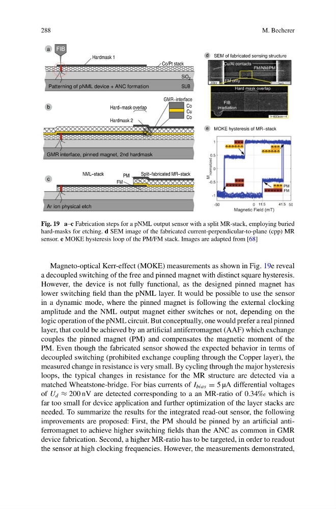
Fig. 19 a–c Fabrication steps for a pNML output sensor with a split MR-stack, employing buried
hard-masks for etching. d SEM image of the fabricated current-perpendicular-to-plane (cpp) MR
sensor. e MOKE hysteresis loop of the PM/FM stack. Images are adapted from [68]
Magneto-optical Kerr-effect (MOKE) measurements as shown in Fig. 19e reveal
a decoupled switching of the free and pinned magnet with distinct square hysteresis.
However, the device is not fully functional, as the designed pinned magnet has
lower switching field than the pNML layer. It would be possible to use the sensor
in a dynamic mode, where the pinned magnet is following the external clocking
amplitude and the NML output magnet either switches or not, depending on the
logic operation of the pNML circuit. But conceptually, one would prefer a real pinned
layer, that could be achieved by an artificial antiferromagnet (AAF) which exchange
couples the pinned magnet (PM) and compensates the magnetic moment of the
PM. Even though the fabricated sensor showed the expected behavior in terms of
decoupled switching (prohibited exchange coupling through the Copper layer), the
measured change in resistance is very small. By cycling through the major hysteresis
loops, the typical changes in resistance for the MR structure are detected via a
matched Wheatstone-bridge. For bias currents of I bias = 5 µA differential voltages
of U d ≈ 200 nV are detected corresponding to a an MR-ratio of 0.34‰ which is
far too small for device application and further optimization of the layer stacks are
needed. To summarize the results for the integrated read-out sensor, the following
improvements are proposed: First, the PM should be pinned by an artificial antiferromagnet to achieve higher switching fields than the ANC as common in GMR
device fabrication. Second, a higher MR-ratio has to be targeted, in order to readout
the sensor at high clocking frequencies. However, the measurements demonstrated,
M. Becherer
Fig. 19 a–c Fabrication steps for a pNML output sensor with a split MR-stack, employing buried
hard-masks for etching. d SEM image of the fabricated current-perpendicular-to-plane (cpp) MR
sensor. e MOKE hysteresis loop of the PM/FM stack. Images are adapted from [68]
Magneto-optical Kerr-effect (MOKE) measurements as shown in Fig. 19e reveal
a decoupled switching of the free and pinned magnet with distinct square hysteresis.
However, the device is not fully functional, as the designed pinned magnet has
lower switching field than the pNML layer. It would be possible to use the sensor
in a dynamic mode, where the pinned magnet is following the external clocking
amplitude and the NML output magnet either switches or not, depending on the
logic operation of the pNML circuit. But conceptually, one would prefer a real pinned
layer, that could be achieved by an artificial antiferromagnet (AAF) which exchange
couples the pinned magnet (PM) and compensates the magnetic moment of the
PM. Even though the fabricated sensor showed the expected behavior in terms of
decoupled switching (prohibited exchange coupling through the Copper layer), the
measured change in resistance is very small. By cycling through the major hysteresis
loops, the typical changes in resistance for the MR structure are detected via a
matched Wheatstone-bridge. For bias currents of I bias = 5 µA differential voltages
of U d ≈ 200 nV are detected corresponding to a an MR-ratio of 0.34‰ which is
far too small for device application and further optimization of the layer stacks are
needed. To summarize the results for the integrated read-out sensor, the following
improvements are proposed: First, the PM should be pinned by an artificial antiferromagnet to achieve higher switching fields than the ANC as common in GMR
device fabrication. Second, a higher MR-ratio has to be targeted, in order to readout
the sensor at high clocking frequencies. However, the measurements demonstrated,