

284
M. Becherer
4.3 Major Building Blocks of 3D pNML
In the following, the state-of-the-art in 3D pNML devices is briefly reviewed.
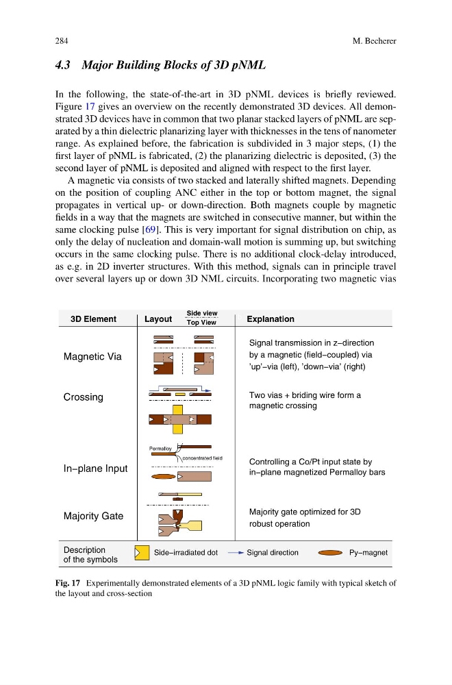
Figure 17 gives an overview on the recently demonstrated 3D devices. All demonstrated 3D devices have in common that two planar stacked layers of pNML are separated by a thin dielectric planarizing layer with thicknesses in the tens of nanometer
range. As explained before, the fabrication is subdivided in 3 major steps, (1) the
first layer of pNML is fabricated, (2) the planarizing dielectric is deposited, (3) the
second layer of pNML is deposited and aligned with respect to the first layer.
A magnetic via consists of two stacked and laterally shifted magnets. Depending
on the position of coupling ANC either in the top or bottom magnet, the signal
propagates in vertical up- or down-direction. Both magnets couple by magnetic
fields in a way that the magnets are switched in consecutive manner, but within the
same clocking pulse [69]. This is very important for signal distribution on chip, as
only the delay of nucleation and domain-wall motion is summing up, but switching
occurs in the same clocking pulse. There is no additional clock-delay introduced,
as e.g. in 2D inverter structures. With this method, signals can in principle travel
over several layers up or down 3D NML circuits. Incorporating two magnetic vias
Majority gate optimized for 3D
robust operation
Side−irradiated dot
Description
of the symbols
Signal direction
Py−magnet
Magnetic Via
Crossing
magnetic crossing
Two vias + briding wire form a
Controlling a Co/Pt input state by
In−plane Input
Majority Gate
in−plane magnetized Permalloy bars
Signal transmission in z−direction
by a magnetic (field−coupled) via
’up’−via (left), ’down−via’ (right)
Top View
Side view
Layout
Explanation
3D Element
concentrated field
Permalloy
b
Fig. 17 Experimentally demonstrated elements of a 3D pNML logic family with typical sketch of
the layout and cross-section
M. Becherer
4.3 Major Building Blocks of 3D pNML
In the following, the state-of-the-art in 3D pNML devices is briefly reviewed.
Figure 17 gives an overview on the recently demonstrated 3D devices. All demonstrated 3D devices have in common that two planar stacked layers of pNML are separated by a thin dielectric planarizing layer with thicknesses in the tens of nanometer
range. As explained before, the fabrication is subdivided in 3 major steps, (1) the
first layer of pNML is fabricated, (2) the planarizing dielectric is deposited, (3) the
second layer of pNML is deposited and aligned with respect to the first layer.
A magnetic via consists of two stacked and laterally shifted magnets. Depending
on the position of coupling ANC either in the top or bottom magnet, the signal
propagates in vertical up- or down-direction. Both magnets couple by magnetic
fields in a way that the magnets are switched in consecutive manner, but within the
same clocking pulse [69]. This is very important for signal distribution on chip, as
only the delay of nucleation and domain-wall motion is summing up, but switching
occurs in the same clocking pulse. There is no additional clock-delay introduced,
as e.g. in 2D inverter structures. With this method, signals can in principle travel
over several layers up or down 3D NML circuits. Incorporating two magnetic vias
Majority gate optimized for 3D
robust operation
Side−irradiated dot
Description
of the symbols
Signal direction
Py−magnet
Magnetic Via
Crossing
magnetic crossing
Two vias + briding wire form a
Controlling a Co/Pt input state by
In−plane Input
Majority Gate
in−plane magnetized Permalloy bars
Signal transmission in z−direction
by a magnetic (field−coupled) via
’up’−via (left), ’down−via’ (right)
Top View
Side view
Layout
Explanation
3D Element
concentrated field
Permalloy
b
Fig. 17 Experimentally demonstrated elements of a 3D pNML logic family with typical sketch of
the layout and cross-section