

3D Nanomagnetic Logic
283
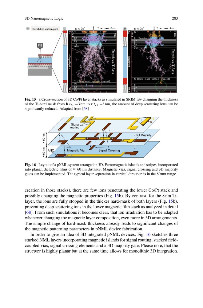
Fig. 15 a Cross-section of 3D Co/Pt layer stacks as simulated in SRIM. By changing the thickness
of the Ti-hard mask from b t T i =3 nm to c t T i =8 nm, the amount of deep scattering ions can be
significantly reduced. Adapted from [68]
S
N
Signal Crossing
~ 60 nm
~ 60 nm
Signal
routing
Magnetic Via
3D Majority
ANC
Fig. 16 Layout of a pNML system arranged in 3D. Ferromagnetic islands and stripes, incorporated
into planar, dielectric films of ≈ 60 nm distance. Magnetic vias, signal crossing and 3D majority
gates can be implemented. The typical layer separation in vertical direction is in the 60 nm range
creation in those stacks), there are few ions penetrating the lower Co/Pt stack and
possibly changing the magnetic properties (Fig. 15b). By contrast, for the 8 nm Tilayer, the ions are fully stopped in the thicker hard-mask of both layers (Fig. 15b),
preventing deep scattering ions in the lower magnetic film stack as analyzed in detail
[68]. From such simulations it becomes clear, that ion irradiation has to be adapted
whenever changing the magnetic layer composition, even more in 3D arrangements.
The simple change of hard-mask thickness already leads to significant changes of
the magnetic patterning parameters in pNML device fabrication.
In order to give an idea of 3D integrated pNML devices, Fig. 16 sketches three
stacked NML layers incorporating magnetic islands for signal routing, stacked fieldcoupled vias, signal crossing elements and a 3D majority gate. Please note, that the
structure is highly planar but at the same time allows for monolithic 3D integration.
283
Fig. 15 a Cross-section of 3D Co/Pt layer stacks as simulated in SRIM. By changing the thickness
of the Ti-hard mask from b t T i =3 nm to c t T i =8 nm, the amount of deep scattering ions can be
significantly reduced. Adapted from [68]
S
N
Signal Crossing
~ 60 nm
~ 60 nm
Signal
routing
Magnetic Via
3D Majority
ANC
Fig. 16 Layout of a pNML system arranged in 3D. Ferromagnetic islands and stripes, incorporated
into planar, dielectric films of ≈ 60 nm distance. Magnetic vias, signal crossing and 3D majority
gates can be implemented. The typical layer separation in vertical direction is in the 60 nm range
creation in those stacks), there are few ions penetrating the lower Co/Pt stack and
possibly changing the magnetic properties (Fig. 15b). By contrast, for the 8 nm Tilayer, the ions are fully stopped in the thicker hard-mask of both layers (Fig. 15b),
preventing deep scattering ions in the lower magnetic film stack as analyzed in detail
[68]. From such simulations it becomes clear, that ion irradiation has to be adapted
whenever changing the magnetic layer composition, even more in 3D arrangements.
The simple change of hard-mask thickness already leads to significant changes of
the magnetic patterning parameters in pNML device fabrication.
In order to give an idea of 3D integrated pNML devices, Fig. 16 sketches three
stacked NML layers incorporating magnetic islands for signal routing, stacked fieldcoupled vias, signal crossing elements and a 3D majority gate. Please note, that the
structure is highly planar but at the same time allows for monolithic 3D integration.