

282
M. Becherer
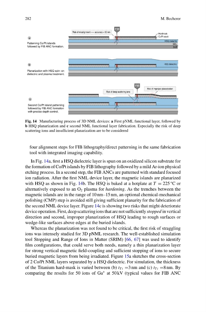
Fig. 14 Manufacturing process of 3D NML devices: a First pNML functional layer, followed by
b HSQ planarization and c second NML functional layer fabrication. Especially the risk of deep
scattering ions and insufficient planarization are to be considered
four alignment steps for FIB lithography/direct patterning in the same fabrication
tool with integrated imaging capability.
In Fig. 14a, first a HSQ dielectric layer is spun on an oxidized silicon substrate for
the formation of Co/Pt islands by FIB lithography followed by a mild Ar-ion physical
etching process. In a second step, the FIB ANCs are patterned with standard focused
ion radiation. After the first NML device layer, the magnetic islands are planarized
with HSQ as shown in Fig. 14b. The HSQ is baked at a hotplate at T = 225
◦ C or
alternatively exposed to an O 2 plasma for hardening. As the trenches between the
magnetic islands are in the range of 10 nm–15 nm, an optional chemical-mechanical
polishing (CMP) step is avoided still giving sufficient planarity for the fabrication of
the second NML device layer. Figure 14c is showing two risks that might deteriorate
device operation. First, deep scattering ions that are not sufficiently stopped in vertical
direction and second, improper planarization of HSQ leading to rough surfaces or
wedge-like surfaces above edges at the buried islands.
Whereas the planarization was not found to be critical, the first risk of straggling
ions was intensely studied for 3D pNML research. The well-established simulation
tool Stopping and Range of Ions in Matter (SRIM) [66, 67] was used to identify
film configurations, that could serve both needs, namely a thin planarization layer
for strong vertical magnetic field-coupling and sufficient stopping of ions to secure
buried magnetic layers from being irradiated. Figure 15a sketches the cross-section
of 2 Co/Pt NML layers separated by a HSQ dielectric. For simulation, the thickness
of the Titanium hard-mask is varied between (b) t T i =3 nm and (c) t T i =8 nm. By
comparing the results for 50 ions of Ga
+ at 50 kV (typical values for FIB ANC
M. Becherer
Fig. 14 Manufacturing process of 3D NML devices: a First pNML functional layer, followed by
b HSQ planarization and c second NML functional layer fabrication. Especially the risk of deep
scattering ions and insufficient planarization are to be considered
four alignment steps for FIB lithography/direct patterning in the same fabrication
tool with integrated imaging capability.
In Fig. 14a, first a HSQ dielectric layer is spun on an oxidized silicon substrate for
the formation of Co/Pt islands by FIB lithography followed by a mild Ar-ion physical
etching process. In a second step, the FIB ANCs are patterned with standard focused
ion radiation. After the first NML device layer, the magnetic islands are planarized
with HSQ as shown in Fig. 14b. The HSQ is baked at a hotplate at T = 225
◦ C or
alternatively exposed to an O 2 plasma for hardening. As the trenches between the
magnetic islands are in the range of 10 nm–15 nm, an optional chemical-mechanical
polishing (CMP) step is avoided still giving sufficient planarity for the fabrication of
the second NML device layer. Figure 14c is showing two risks that might deteriorate
device operation. First, deep scattering ions that are not sufficiently stopped in vertical
direction and second, improper planarization of HSQ leading to rough surfaces or
wedge-like surfaces above edges at the buried islands.
Whereas the planarization was not found to be critical, the first risk of straggling
ions was intensely studied for 3D pNML research. The well-established simulation
tool Stopping and Range of Ions in Matter (SRIM) [66, 67] was used to identify
film configurations, that could serve both needs, namely a thin planarization layer
for strong vertical magnetic field-coupling and sufficient stopping of ions to secure
buried magnetic layers from being irradiated. Figure 15a sketches the cross-section
of 2 Co/Pt NML layers separated by a HSQ dielectric. For simulation, the thickness
of the Titanium hard-mask is varied between (b) t T i =3 nm and (c) t T i =8 nm. By
comparing the results for 50 ions of Ga
+ at 50 kV (typical values for FIB ANC