

3D Nanomagnetic Logic
261
ability. This has already been pursued by ferromagnetic logic device implementations of different flavors. In order to distinguish our approach from other magnetic
device implementations, we restrict ourselves to the following preconditions:
• Boolean algebra with non-volatile binary states (digital information processing)
from ferromagnetic entities. The binary states encode logic ‘0’ and ‘1’.
• Planar fabrication with standard microelectronic equipment (top-down approach),
compatible with CMOS, beneficially as a back-end of line (BEOL) process with
low temperature budget.
• No electrical current flow except for in-/output interfaces, latching/synchronization
of signals (sequential logic) and clocking circuitry for power supply.
The main implementations fulfilling these conditions are:
1. Magnetic domain-wall (DW)-logic, e.g. [8].
2. In-plane Nanomagnetic Logic (iNML) [9–13].
3. Perpendicular Nanomagnetic Logic (pNML) [14–18].
For (1) DW-logic the reader is referred to detailed descriptions in e.g. [8], for
(2) In-plane Nanomagnetic Logic e.g. [11, 13]. This book chapter will exclusively
focus on (3) pNML devices and circuits composed of magnetic multilayers with
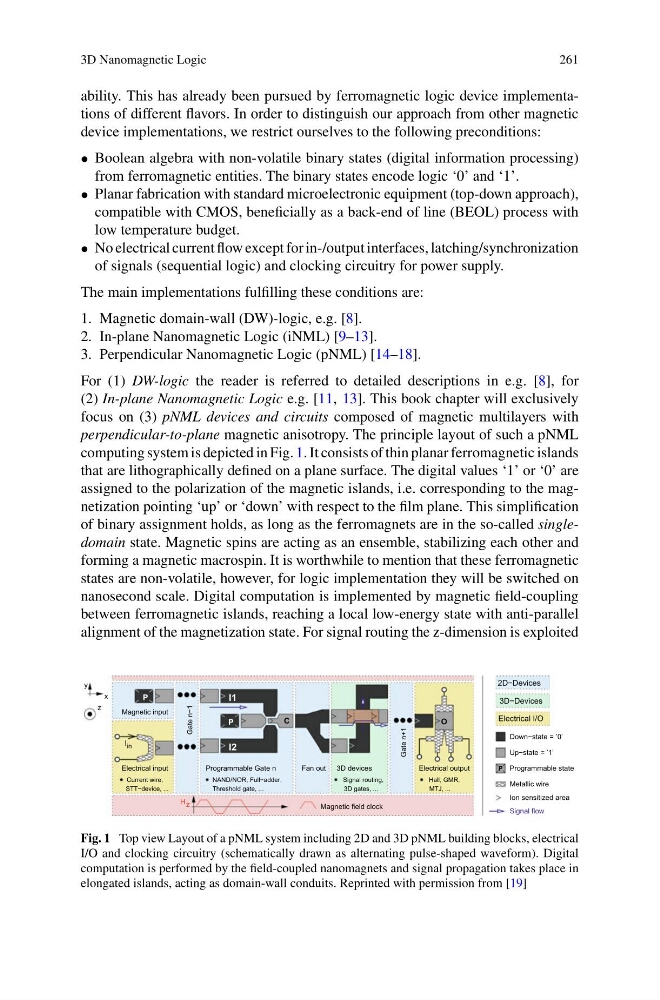
perpendicular-to-plane magnetic anisotropy. The principle layout of such a pNML
computing system is depicted in Fig. 1. It consists of thin planar ferromagnetic islands
that are lithographically defined on a plane surface. The digital values ‘1’ or ‘0’ are
assigned to the polarization of the magnetic islands, i.e. corresponding to the magnetization pointing ‘up’ or ‘down’ with respect to the film plane. This simplification
of binary assignment holds, as long as the ferromagnets are in the so-called singledomain state. Magnetic spins are acting as an ensemble, stabilizing each other and
forming a magnetic macrospin. It is worthwhile to mention that these ferromagnetic
states are non-volatile, however, for logic implementation they will be switched on
nanosecond scale. Digital computation is implemented by magnetic field-coupling
between ferromagnetic islands, reaching a local low-energy state with anti-parallel
alignment of the magnetization state. For signal routing the z-dimension is exploited
I in
Magnetic field clock
x
y
z
2D−Devices
3D−Devices
Electrical I/O
Down−state = ’0’
Metallic wire
Up−state = ’1’
Programmable state
Signal flow
Ion sensitized area
Magnetic input
Gate n+1
Threshold gate, ...
NAND/NOR, Full−adder,
Electrical input
3D devices
Signal routing,
3D gates, ...
t
u
p
t
u
o
l
a
c
i
r
t
c
e
l
E
t
u
o
n
a
F
Hall, GMR,
MTJ, ...
Current wire,
STT−device, ...
Gate n−1
Programmable Gate n
I2
I1
H z
P
P
P
C
O
Fig. 1 Top view Layout of a pNML system including 2D and 3D pNML building blocks, electrical
I/O and clocking circuitry (schematically drawn as alternating pulse-shaped waveform). Digital
computation is performed by the field-coupled nanomagnets and signal propagation takes place in
elongated islands, acting as domain-wall conduits. Reprinted with permission from [19]
261
ability. This has already been pursued by ferromagnetic logic device implementations of different flavors. In order to distinguish our approach from other magnetic
device implementations, we restrict ourselves to the following preconditions:
• Boolean algebra with non-volatile binary states (digital information processing)
from ferromagnetic entities. The binary states encode logic ‘0’ and ‘1’.
• Planar fabrication with standard microelectronic equipment (top-down approach),
compatible with CMOS, beneficially as a back-end of line (BEOL) process with
low temperature budget.
• No electrical current flow except for in-/output interfaces, latching/synchronization
of signals (sequential logic) and clocking circuitry for power supply.
The main implementations fulfilling these conditions are:
1. Magnetic domain-wall (DW)-logic, e.g. [8].
2. In-plane Nanomagnetic Logic (iNML) [9–13].
3. Perpendicular Nanomagnetic Logic (pNML) [14–18].
For (1) DW-logic the reader is referred to detailed descriptions in e.g. [8], for
(2) In-plane Nanomagnetic Logic e.g. [11, 13]. This book chapter will exclusively
focus on (3) pNML devices and circuits composed of magnetic multilayers with
perpendicular-to-plane magnetic anisotropy. The principle layout of such a pNML
computing system is depicted in Fig. 1. It consists of thin planar ferromagnetic islands
that are lithographically defined on a plane surface. The digital values ‘1’ or ‘0’ are
assigned to the polarization of the magnetic islands, i.e. corresponding to the magnetization pointing ‘up’ or ‘down’ with respect to the film plane. This simplification
of binary assignment holds, as long as the ferromagnets are in the so-called singledomain state. Magnetic spins are acting as an ensemble, stabilizing each other and
forming a magnetic macrospin. It is worthwhile to mention that these ferromagnetic
states are non-volatile, however, for logic implementation they will be switched on
nanosecond scale. Digital computation is implemented by magnetic field-coupling
between ferromagnetic islands, reaching a local low-energy state with anti-parallel
alignment of the magnetization state. For signal routing the z-dimension is exploited
I in
Magnetic field clock
x
y
z
2D−Devices
3D−Devices
Electrical I/O
Down−state = ’0’
Metallic wire
Up−state = ’1’
Programmable state
Signal flow
Ion sensitized area
Magnetic input
Gate n+1
Threshold gate, ...
NAND/NOR, Full−adder,
Electrical input
3D devices
Signal routing,
3D gates, ...
t
u
p
t
u
o
l
a
c
i
r
t
c
e
l
E
t
u
o
n
a
F
Hall, GMR,
MTJ, ...
Current wire,
STT−device, ...
Gate n−1
Programmable Gate n
I2
I1
H z
P
P
P
C
O
Fig. 1 Top view Layout of a pNML system including 2D and 3D pNML building blocks, electrical
I/O and clocking circuitry (schematically drawn as alternating pulse-shaped waveform). Digital
computation is performed by the field-coupled nanomagnets and signal propagation takes place in
elongated islands, acting as domain-wall conduits. Reprinted with permission from [19]