

222
T. T.-H. Kim
MUX
MUX
VDD
Bit
Ref
(high)
Ref
(low)
REF
REF
Test
Mode
OUT
OUTB
I B
I H
I L
(I H +I L )/2
P1
P2
P3
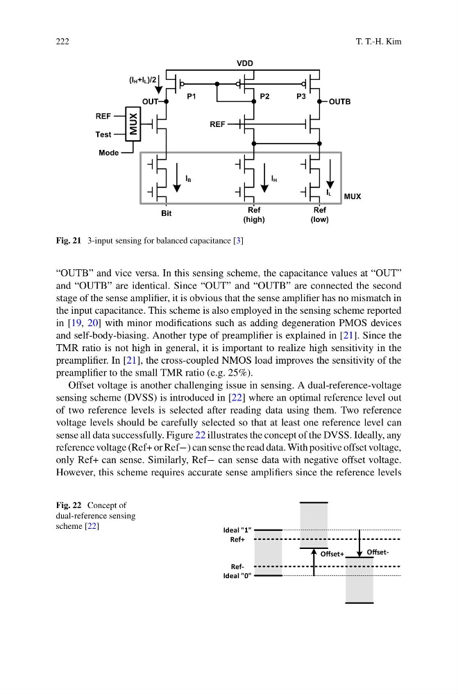
Fig. 21 3-input sensing for balanced capacitance [3]
“OUTB” and vice versa. In this sensing scheme, the capacitance values at “OUT”
and “OUTB” are identical. Since “OUT” and “OUTB” are connected the second
stage of the sense amplifier, it is obvious that the sense amplifier has no mismatch in
the input capacitance. This scheme is also employed in the sensing scheme reported
in [19, 20] with minor modifications such as adding degeneration PMOS devices
and self-body-biasing. Another type of preamplifier is explained in [21]. Since the
TMR ratio is not high in general, it is important to realize high sensitivity in the
preamplifier. In [21], the cross-coupled NMOS load improves the sensitivity of the
preamplifier to the small TMR ratio (e.g. 25%).
Offset voltage is another challenging issue in sensing. A dual-reference-voltage
sensing scheme (DVSS) is introduced in [22] where an optimal reference level out
of two reference levels is selected after reading data using them. Two reference
voltage levels should be carefully selected so that at least one reference level can
sense all data successfully. Figure 22 illustrates the concept of the DVSS. Ideally, any
reference voltage (Ref+ or Ref−) can sense the read data. With positive offset voltage,
only Ref+ can sense. Similarly, Ref− can sense data with negative offset voltage.
However, this scheme requires accurate sense amplifiers since the reference levels
Fig. 22 Concept of
dual-reference sensing
scheme [22]
Ideal "1"
Ideal "0"
Ref+
RefOffset+
Offset-
T. T.-H. Kim
MUX
MUX
VDD
Bit
Ref
(high)
Ref
(low)
REF
REF
Test
Mode
OUT
OUTB
I B
I H
I L
(I H +I L )/2
P1
P2
P3
Fig. 21 3-input sensing for balanced capacitance [3]
“OUTB” and vice versa. In this sensing scheme, the capacitance values at “OUT”
and “OUTB” are identical. Since “OUT” and “OUTB” are connected the second
stage of the sense amplifier, it is obvious that the sense amplifier has no mismatch in
the input capacitance. This scheme is also employed in the sensing scheme reported
in [19, 20] with minor modifications such as adding degeneration PMOS devices
and self-body-biasing. Another type of preamplifier is explained in [21]. Since the
TMR ratio is not high in general, it is important to realize high sensitivity in the
preamplifier. In [21], the cross-coupled NMOS load improves the sensitivity of the
preamplifier to the small TMR ratio (e.g. 25%).
Offset voltage is another challenging issue in sensing. A dual-reference-voltage
sensing scheme (DVSS) is introduced in [22] where an optimal reference level out
of two reference levels is selected after reading data using them. Two reference
voltage levels should be carefully selected so that at least one reference level can
sense all data successfully. Figure 22 illustrates the concept of the DVSS. Ideally, any
reference voltage (Ref+ or Ref−) can sense the read data. With positive offset voltage,
only Ref+ can sense. Similarly, Ref− can sense data with negative offset voltage.
However, this scheme requires accurate sense amplifiers since the reference levels
Fig. 22 Concept of
dual-reference sensing
scheme [22]
Ideal "1"
Ideal "0"
Ref+
RefOffset+
Offset-