

Circuit Design for Non-volatile Magnetic Memory
221
[17]. Since this scheme has no write operation, the overall read latency and power
consumption can be significantly improved compared to the previous self-reference
scheme.
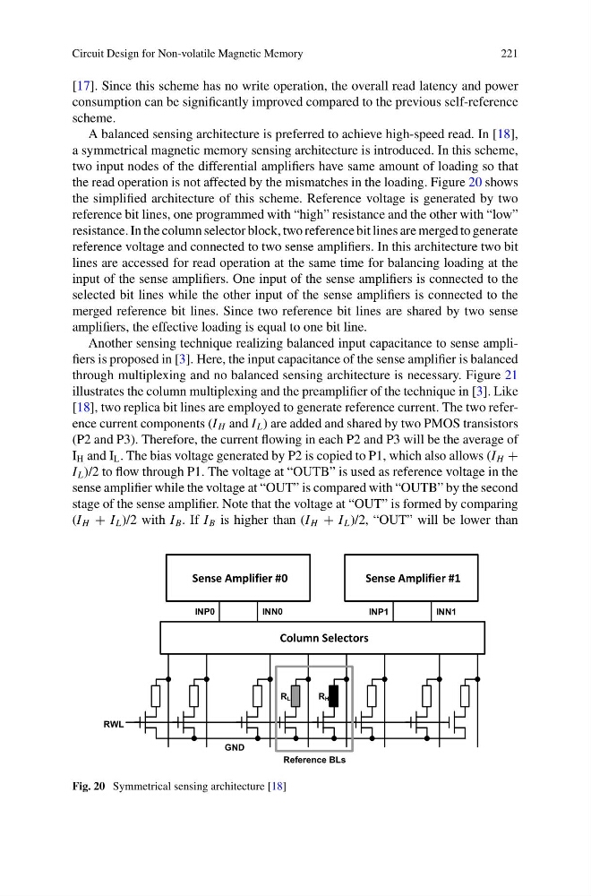
A balanced sensing architecture is preferred to achieve high-speed read. In [18],
a symmetrical magnetic memory sensing architecture is introduced. In this scheme,
two input nodes of the differential amplifiers have same amount of loading so that
the read operation is not affected by the mismatches in the loading. Figure 20 shows
the simplified architecture of this scheme. Reference voltage is generated by two
reference bit lines, one programmed with “high” resistance and the other with “low”
resistance. In the column selector block, two reference bit lines are merged to generate
reference voltage and connected to two sense amplifiers. In this architecture two bit
lines are accessed for read operation at the same time for balancing loading at the
input of the sense amplifiers. One input of the sense amplifiers is connected to the
selected bit lines while the other input of the sense amplifiers is connected to the
merged reference bit lines. Since two reference bit lines are shared by two sense
amplifiers, the effective loading is equal to one bit line.
Another sensing technique realizing balanced input capacitance to sense amplifiers is proposed in [3]. Here, the input capacitance of the sense amplifier is balanced
through multiplexing and no balanced sensing architecture is necessary. Figure 21
illustrates the column multiplexing and the preamplifier of the technique in [3]. Like
[18], two replica bit lines are employed to generate reference current. The two reference current components (I H and I L ) are added and shared by two PMOS transistors
(P2 and P3). Therefore, the current flowing in each P2 and P3 will be the average of
I H and I L . The bias voltage generated by P2 is copied to P1, which also allows (I H +
I L )/2 to flow through P1. The voltage at “OUTB” is used as reference voltage in the
sense amplifier while the voltage at “OUT” is compared with “OUTB” by the second
stage of the sense amplifier. Note that the voltage at “OUT” is formed by comparing
(I H + I L )/2 with I B . If I B is higher than (I H + I L )/2, “OUT” will be lower than
Sense Amplifier #0
RWL
GND
Sense Amplifier #1
Column Selectors
RL
RH
Reference BLs
INP0
INN0
INP1
INN1
Fig. 20 Symmetrical sensing architecture [18]
221
[17]. Since this scheme has no write operation, the overall read latency and power
consumption can be significantly improved compared to the previous self-reference
scheme.
A balanced sensing architecture is preferred to achieve high-speed read. In [18],
a symmetrical magnetic memory sensing architecture is introduced. In this scheme,
two input nodes of the differential amplifiers have same amount of loading so that
the read operation is not affected by the mismatches in the loading. Figure 20 shows
the simplified architecture of this scheme. Reference voltage is generated by two
reference bit lines, one programmed with “high” resistance and the other with “low”
resistance. In the column selector block, two reference bit lines are merged to generate
reference voltage and connected to two sense amplifiers. In this architecture two bit
lines are accessed for read operation at the same time for balancing loading at the
input of the sense amplifiers. One input of the sense amplifiers is connected to the
selected bit lines while the other input of the sense amplifiers is connected to the
merged reference bit lines. Since two reference bit lines are shared by two sense
amplifiers, the effective loading is equal to one bit line.
Another sensing technique realizing balanced input capacitance to sense amplifiers is proposed in [3]. Here, the input capacitance of the sense amplifier is balanced
through multiplexing and no balanced sensing architecture is necessary. Figure 21
illustrates the column multiplexing and the preamplifier of the technique in [3]. Like
[18], two replica bit lines are employed to generate reference current. The two reference current components (I H and I L ) are added and shared by two PMOS transistors
(P2 and P3). Therefore, the current flowing in each P2 and P3 will be the average of
I H and I L . The bias voltage generated by P2 is copied to P1, which also allows (I H +
I L )/2 to flow through P1. The voltage at “OUTB” is used as reference voltage in the
sense amplifier while the voltage at “OUT” is compared with “OUTB” by the second
stage of the sense amplifier. Note that the voltage at “OUT” is formed by comparing
(I H + I L )/2 with I B . If I B is higher than (I H + I L )/2, “OUT” will be lower than
Sense Amplifier #0
RWL
GND
Sense Amplifier #1
Column Selectors
RL
RH
Reference BLs
INP0
INN0
INP1
INN1
Fig. 20 Symmetrical sensing architecture [18]