

Circuit Design for Non-volatile Magnetic Memory
215
becomes high (i.e. DONE = “1”) and the write operation ends. In [5], the VOW
scheme achieved the write latency improvement of 52% and the energy saving of
29% compared to the conventional fixed pulse write scheme.
The VEW scheme is another probabilistic design technique for addressing the
stochastic switching features of the STT MRAMs [6]. In this scheme, the write
pulse ends when a successful write operation is achieved by monitoring the status
of an STT MRAM cell during write operation. This scheme significantly reduces
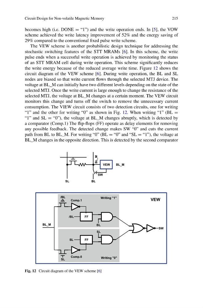
the write energy because of the reduced average write time. Figure 12 shows the
circuit diagram of the VEW scheme [6]. During write operation, the BL and SL
nodes are biased so that write current flows through the selected MTJ device. The
voltage at BL_M can initially have two different levels depending on the state of the
selected MTJ. Once the write current is large enough to change the resistance of the
selected MTJ, the voltage at BL_M changes at a certain moment. The VEW circuit
monitors this change and turns off the switch to remove the unnecessary current
consumption. The VIEW circuit consists of two detection circuits, one for writing
“1” and the other for writing “0” as shown in Fig. 12. When writing “1” (BL =
“1” and SL = “0”), the voltage at BL_M changes abruptly, which is detected by
a comparator (Comp.1) The flip-flops (FF) operate as delay elements for removing
any possible feedback. The detected change makes SW “0” and cuts the current
path from BL to BL_M. For writing “0” (BL = “0” and “SL = “1”), the voltage at
BL_M changes in the opposite direction. This is detected by the second comparator
BL_M
SL
BL
VEW
SW
BL_M
FF
BL
SW
/BL
FF
SL
SL
/BL
SL
Writing "1"
Writing "0"
BL_M
VEW
Comp.1
Comp.0
Fig. 12 Circuit diagram of the VEW scheme [6]
215
becomes high (i.e. DONE = “1”) and the write operation ends. In [5], the VOW
scheme achieved the write latency improvement of 52% and the energy saving of
29% compared to the conventional fixed pulse write scheme.
The VEW scheme is another probabilistic design technique for addressing the
stochastic switching features of the STT MRAMs [6]. In this scheme, the write
pulse ends when a successful write operation is achieved by monitoring the status
of an STT MRAM cell during write operation. This scheme significantly reduces
the write energy because of the reduced average write time. Figure 12 shows the
circuit diagram of the VEW scheme [6]. During write operation, the BL and SL
nodes are biased so that write current flows through the selected MTJ device. The
voltage at BL_M can initially have two different levels depending on the state of the
selected MTJ. Once the write current is large enough to change the resistance of the
selected MTJ, the voltage at BL_M changes at a certain moment. The VEW circuit
monitors this change and turns off the switch to remove the unnecessary current
consumption. The VIEW circuit consists of two detection circuits, one for writing
“1” and the other for writing “0” as shown in Fig. 12. When writing “1” (BL =
“1” and SL = “0”), the voltage at BL_M changes abruptly, which is detected by
a comparator (Comp.1) The flip-flops (FF) operate as delay elements for removing
any possible feedback. The detected change makes SW “0” and cuts the current
path from BL to BL_M. For writing “0” (BL = “0” and “SL = “1”), the voltage at
BL_M changes in the opposite direction. This is detected by the second comparator
BL_M
SL
BL
VEW
SW
BL_M
FF
BL
SW
/BL
FF
SL
SL
/BL
SL
Writing "1"
Writing "0"
BL_M
VEW
Comp.1
Comp.0
Fig. 12 Circuit diagram of the VEW scheme [6]