

214
T. T.-H. Kim
write pulse width can be adaptively changed to enhance the overall system performance. In [5], the optimal pulse width is based on Hamming weight. The optimal
pulse width values for various Hamming weights at different temperatures are stored
in a look-up table. The WRAP scheme demonstrated the write latency improvement
of 40% and the energy saving of 26% when compared to the conventional fixed pulse
write scheme. Figure 10 illustrates the system diagram of the WRAP scheme.
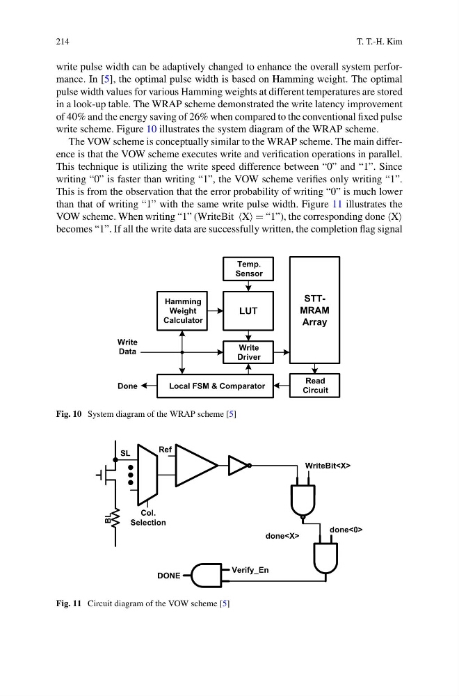
The VOW scheme is conceptually similar to the WRAP scheme. The main difference is that the VOW scheme executes write and verification operations in parallel.
This technique is utilizing the write speed difference between “0” and “1”. Since
writing “0” is faster than writing “1”, the VOW scheme verifies only writing “1”.
This is from the observation that the error probability of writing “0” is much lower
than that of writing “1” with the same write pulse width. Figure 11 illustrates the
VOW scheme. When writing “1” (WriteBit = “1”), the corresponding done
becomes “1”. If all the write data are successfully written, the completion flag signal
Hamming
Weight
Calculator
LUT
Temp.
Sensor
Write
Driver
STTMRAM
Array
Read
Circuit
Local FSM & Comparator
Done
Write
Data
Fig. 10 System diagram of the WRAP scheme [5]
BL
Col.
Selection
SL
Ref
WriteBit
done
done<0>
Verify_En
DONE
Fig. 11 Circuit diagram of the VOW scheme [5]
T. T.-H. Kim
write pulse width can be adaptively changed to enhance the overall system performance. In [5], the optimal pulse width is based on Hamming weight. The optimal
pulse width values for various Hamming weights at different temperatures are stored
in a look-up table. The WRAP scheme demonstrated the write latency improvement
of 40% and the energy saving of 26% when compared to the conventional fixed pulse
write scheme. Figure 10 illustrates the system diagram of the WRAP scheme.
The VOW scheme is conceptually similar to the WRAP scheme. The main difference is that the VOW scheme executes write and verification operations in parallel.
This technique is utilizing the write speed difference between “0” and “1”. Since
writing “0” is faster than writing “1”, the VOW scheme verifies only writing “1”.
This is from the observation that the error probability of writing “0” is much lower
than that of writing “1” with the same write pulse width. Figure 11 illustrates the
VOW scheme. When writing “1” (WriteBit = “1”), the corresponding done
becomes “1”. If all the write data are successfully written, the completion flag signal
Hamming
Weight
Calculator
LUT
Temp.
Sensor
Write
Driver
STTMRAM
Array
Read
Circuit
Local FSM & Comparator
Done
Write
Data
Fig. 10 System diagram of the WRAP scheme [5]
BL
Col.
Selection
SL
Ref
WriteBit
done
done<0>
Verify_En
DONE
Fig. 11 Circuit diagram of the VOW scheme [5]