

Circuit Design for Non-volatile Magnetic Memory
213
PreCh.
PreCh.
Source
(On)
Source
(Off)
Sink
(Off)
Sink
(On)
Thick Oxide TRs
Col. Dec.
Col. Dec.
Array
BL
Dec
Gate
Source
(a)
Dec.
PreCh.
Gate
Source
VDD
~2× VDD
VDD
>VDD
VDD
(b)
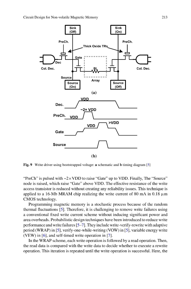
Fig. 9 Write driver using bootstrapped voltage: a schematic and b timing diagram [5]
“PreCh” is pulsed with ~2×VDD to raise “Gate” up to VDD. Finally, The “Source”
node is raised, which raise “Gate” above VDD. The effective resistance of the write
access transistor is reduced without creating any reliability issues. This technique is
applied to a 16-Mb MRAM chip realizing the write current of 80 mA in 0.18 µm
CMOS technology.
Programming magnetic memory is a stochastic process because of the random
thermal fluctuations [5]. Therefore, it is challenging to remove write failures using
a conventional fixed write current scheme without inducing significant power and
area overheads. Probabilistic design techniques have been introduced to reduce write
performance and write failures [5–7]. They include write-verify-rewrite with adaptive
period (WRAP) in [5], verify-one-while-writing (VOW) in [5], variable energy write
(VEW) in [6], and self-timed write operation in [7].
In the WRAP scheme, each write operation is followed by a read operation. Then,
the read data is compared with the write data to decide whether to execute a rewrite
operation. This iteration is repeated until the write operation is successful. Here, the
213
PreCh.
PreCh.
Source
(On)
Source
(Off)
Sink
(Off)
Sink
(On)
Thick Oxide TRs
Col. Dec.
Col. Dec.
Array
BL
Dec
Gate
Source
(a)
Dec.
PreCh.
Gate
Source
VDD
~2× VDD
VDD
>VDD
VDD
(b)
Fig. 9 Write driver using bootstrapped voltage: a schematic and b timing diagram [5]
“PreCh” is pulsed with ~2×VDD to raise “Gate” up to VDD. Finally, The “Source”
node is raised, which raise “Gate” above VDD. The effective resistance of the write
access transistor is reduced without creating any reliability issues. This technique is
applied to a 16-Mb MRAM chip realizing the write current of 80 mA in 0.18 µm
CMOS technology.
Programming magnetic memory is a stochastic process because of the random
thermal fluctuations [5]. Therefore, it is challenging to remove write failures using
a conventional fixed write current scheme without inducing significant power and
area overheads. Probabilistic design techniques have been introduced to reduce write
performance and write failures [5–7]. They include write-verify-rewrite with adaptive
period (WRAP) in [5], verify-one-while-writing (VOW) in [5], variable energy write
(VEW) in [6], and self-timed write operation in [7].
In the WRAP scheme, each write operation is followed by a read operation. Then,
the read data is compared with the write data to decide whether to execute a rewrite
operation. This iteration is repeated until the write operation is successful. Here, the